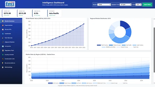
The global semiconductor lift-off resists market is projected to grow from USD 1,677.7 million in 2025 to approximately USD 3,490 million by 2035, recording an absolute increase of USD 1,812.3 million over the forecast period. This translates into a total growth of 108.0%, with the market forecast to expand at a compound annual growth rate (CAGR) of 7.6% between 2025 and 2035. The overall market size is expected to grow by nearly 2.1X during the same period, supported by increasing advanced semiconductor manufacturing investments, growing demand for precision photolithography materials in sub-micron patterning applications, and rising adoption of specialized resist formulations across compound semiconductor devices and photonic integrated circuits requiring exceptional pattern transfer capabilities.
The market demonstrates robust expansion across both established and emerging semiconductor manufacturing regions, with microelectronics fabrication applications maintaining dominant positioning throughout the forecast period. Growth is particularly pronounced in Asia Pacific markets where leading-edge semiconductor fabs and advanced packaging facilities are establishing comprehensive photolithography capabilities requiring specialized lift-off resist systems. North American and European markets continue expanding through compound semiconductor manufacturing development and photonics device production programs, while emerging markets demonstrate accelerating adoption rates driven by semiconductor industry localization initiatives and advanced electronics manufacturing facility development supporting technological self-sufficiency objectives.
Lift-off resist technology maintains critical positioning within semiconductor manufacturing through enabling precise metal pattern formation without etching damage to underlying sensitive layers, particularly essential for compound semiconductors including gallium arsenide and gallium nitride devices where wet or dry etching can compromise material properties. The process proves indispensable for advanced packaging applications including flip-chip bumping, wafer-level packaging, and through-silicon via metallization requiring thick metal deposits with precise pattern definition. Market expansion reflects broader semiconductor industry trends toward heterogeneous integration, advanced packaging complexity growth, and photonic device proliferation supporting optical communications infrastructure and emerging quantum computing applications requiring specialized fabrication materials delivering exceptional process control and material compatibility.
![]()
| Metric | Value |
|---|---|
| Market Value (2025) | USD 1,677.7 million |
| Market Forecast Value (2035) | USD 3,490 million |
| Forecast CAGR (2025-2035) | 7.6% |
| ADVANCED SEMICONDUCTOR MANUFACTURING | PHOTOLITHOGRAPHY TECHNOLOGY REQUIREMENTS | MATERIAL INNOVATION STANDARDS |
|---|---|---|
| Leading-Edge Fab Investment Manufacturing capacity expansion across advanced semiconductor nodes driving demand for specialized photolithography materials supporting precision patterning. Compound Semiconductor Development Development of gallium nitride and silicon carbide power devices requiring lift-off processes preventing etching damage to sensitive epitaxial layers. Advanced Packaging Growth Expansion of heterogeneous integration and 3D packaging technologies establishing lift-off processes for complex metallization patterns. | Sub-Micron Pattern Requirements Modern semiconductor manufacturing demands resist materials delivering exceptional resolution and pattern transfer fidelity for critical dimension control. Undercut Profile Control Fabrication processes requiring specialized resist profiles enabling clean metal lift-off without pattern damage or residue formation. Multi-Layer Processing Advanced devices implementing complex resist stacks necessitating materials with precise thickness control and inter-layer compatibility. | Process Integration Standards Manufacturing protocols establishing performance benchmarks requiring validated resist formulations with documented process windows. Material Purity Requirements Quality standards demanding ultra-high purity resist materials preventing contamination and defect formation throughout semiconductor processing. Environmental Compliance Regulatory frameworks driving development of environmentally responsible resist chemistries reducing hazardous material usage throughout photolithography operations. |
| Category | Segments Covered |
|---|---|
| By Resist Type | Positive Tone Lift-off Resists, Negative Tone Lift-off Resists, Others |
| By Application | Microelectronics Fabrication, Photonic Devices and Circuits, Others |
| By Region | North America, Europe, Asia Pacific, Latin America, Middle East & Africa |
![]()
| Segment | 2025 to 2035 Outlook |
|---|---|
| Positive Tone Lift-off Resists | Leader in 2025 with 67.4% market share; maintains leadership through 2035. Dominant presence in advanced semiconductor fabrication, established process integration protocols, proven reliability for sub-micron patterning applications. Serves IC manufacturing, compound semiconductor devices, and advanced packaging requiring undercut profile formation. Momentum: steady growth through leading-edge fab expansion and compound semiconductor development. Superior undercut formation characteristics and established track record support continued adoption. Chemical amplification systems enable high sensitivity supporting advanced lithography tools. Watchouts: solvent compatibility requirements, process temperature constraints affecting some applications. |
| Negative Tone Lift-off Resists | Growing segment benefiting from advanced packaging applications and thick resist requirements. Specialized applications including high-aspect-ratio structures, thick metal deposition processes, and specific device geometries. Serves flip-chip bumping, through-silicon via formation, and MEMS device fabrication. Momentum: rising adoption in advanced packaging and 3D integration applications requiring thick resist capabilities. Image reversal processes enable undercut formation in negative tone systems. Beneficial for applications requiring superior adhesion and chemical resistance. Watchouts: limited resolution versus positive systems, processing complexity for undercut formation. |
| Others | Niche segment including hybrid resist systems, specialty formulations, and emerging resist chemistries. Custom materials addressing specific process challenges and novel device architectures. Momentum: selective growth driven by specialized applications requiring unique material properties. Includes dual-tone resists, dissolution rate modifiers, and experimental chemistries supporting research applications. Limited market presence due to established positive tone dominance. |
![]()
| Segment | 2025 to 2035 Outlook |
|---|---|
| Microelectronics Fabrication | Dominant application with 71.2% market share in 2025, driven by advanced semiconductor manufacturing expansion and integrated circuit complexity growth. Serves logic device fabrication, memory chip production, compound semiconductor manufacturing, and power electronics requiring precision metal patterning. Lift-off processes essential for gate metallization, interconnect formation, and contact pad fabrication across diverse device architectures. Momentum: strong growth through leading-edge node transitions, compound semiconductor device development, and advanced packaging proliferation. Process advantages including damage-free patterning and material compatibility drive continued adoption. Watchouts: process cost pressures, alternative patterning technology competition for specific applications. |
| Photonic Devices and Circuits | Emerging high-growth application segment for optical communications infrastructure, photonic integrated circuits, and quantum photonics device fabrication. Serves silicon photonics manufacturing, III-V photonic devices, and specialty optical components requiring precision metal patterns on optical waveguides and active devices. Lift-off processes critical for metal contact formation without damaging optical structures. Momentum: rapid growth driven by optical communications capacity expansion, data center interconnect requirements, and emerging quantum computing hardware development. Silicon photonics adoption accelerates in telecommunications and high-performance computing applications. Watchouts: specialized process requirements, material compatibility challenges with diverse substrate materials. |
| Others | Diverse applications including MEMS device fabrication, sensor manufacturing, research and development activities, and specialty electronic components. Serves microelectromechanical systems requiring suspended metal structures, biosensor fabrication, and advanced research programs exploring novel device concepts. Momentum: steady demand from specialized manufacturing and research institutions. Applications span diverse technology areas including bioelectronics, flexible electronics, and emerging device architectures requiring precision metal patterning capabilities. |
| DRIVERS | RESTRAINTS | KEY TRENDS |
|---|---|---|
| Advanced Node Transitions Continuing semiconductor technology roadmap progression toward smaller nodes driving demand for advanced photolithography materials with enhanced resolution capabilities. Compound Semiconductor Adoption Expansion of gallium nitride and silicon carbide power electronics requiring lift-off processes preventing etch damage to sensitive device structures. Photonics Infrastructure Growth Increasing emphasis on optical communications and photonic integrated circuits supporting adoption of specialized resist materials throughout device fabrication. | Process Cost Pressures Material costs and process complexity affecting adoption rates in cost-sensitive applications and mature technology nodes. Alternative Technology Competition Damascene metallization and subtractive patterning methods providing competition in specific applications through process simplification. Technical Skill Requirements Specialized process knowledge and optimization expertise creating barriers for facilities lacking experienced photolithography personnel. | Resolution Enhancement Development of advanced resist chemistries with improved resolution capabilities supporting leading-edge lithography tool utilization and critical dimension control. Environmental Formulations Introduction of environmentally responsible resist materials reducing hazardous solvent content and improving waste treatment compatibility. Process Window Expansion Enhanced resist formulations providing broader process latitude, improved defect performance, and simplified process optimization. Multi-Layer Systems Advanced resist stack architectures enabling complex pattern profiles, improved undercut control, and enhanced process capabilities. |
![]()
| Country | CAGR (2025-2035) |
|---|---|
| China | 10.3% |
| India | 9.5% |
| Germany | 8.7% |
| Brazil | 8.0% |
| United States | 7.2% |
![]()
Revenue from semiconductor lift-off resists in China is projected to exhibit strong growth with a market value of USD 633.7 million by 2035, driven by expanding semiconductor manufacturing infrastructure and comprehensive compound semiconductor facility development creating substantial opportunities for photolithography material suppliers across logic fabrication operations, memory production facilities, and power electronics manufacturing requiring advanced resist capabilities. The country's aggressive semiconductor self-sufficiency initiatives and expanding domestic foundry capabilities are creating significant demand for both established positive tone resist systems and specialized negative tone formulations. Major semiconductor manufacturers and compound semiconductor producers are establishing comprehensive fabrication facilities to support technology development and meet growing domestic chip demand.
Revenue from semiconductor lift-off resists in India is expanding to reach USD 290.4 million by 2035, supported by extensive semiconductor manufacturing development programs and comprehensive electronics production facility establishment creating sustained demand for reliable photolithography materials across diverse device categories and technology nodes. The country's ambitious semiconductor industry development initiatives and expanding electronics manufacturing capabilities are driving demand for resist solutions that provide consistent performance while supporting cost-effective facility operations. Material suppliers and semiconductor equipment providers are investing in market development to support growing fabrication capabilities and technology transfer programs.
Demand for semiconductor lift-off resists in Germany is projected to reach USD 290.4 million by 2035, supported by the country's leadership in compound semiconductor manufacturing and advanced photonics technologies requiring sophisticated lift-off resist systems for power device production and optical component fabrication. German semiconductor companies are implementing high-performance resist materials that support advanced device architectures, operational efficiency, and comprehensive process control. The market is characterized by focus on process excellence, material quality, and compliance with stringent semiconductor manufacturing and environmental standards.
Revenue from semiconductor lift-off resists in Brazil is growing to reach USD 163.2 million by 2035, driven by electronics manufacturing development programs and increasing semiconductor industry establishment creating sustained opportunities for photolithography material suppliers serving both established electronics operations and emerging semiconductor fabrication initiatives. The country's expanding electronics manufacturing base and growing technology development awareness are creating demand for resist materials that support diverse processing requirements while maintaining quality standards. Material suppliers and equipment providers are developing distribution strategies to support operational requirements and technology transfer programs.
Demand for semiconductor lift-off resists in United States is projected to reach USD 251.6 million by 2035, expanding at a CAGR of 7.2%, driven by advanced semiconductor manufacturing excellence and compound semiconductor leadership supporting next-generation device development and comprehensive photonics manufacturing applications. The country's established semiconductor industry leadership and growing strategic manufacturing initiatives are creating demand for high-performance resist materials that support technology advancement and manufacturing capability. Material manufacturers and photolithography equipment suppliers are maintaining comprehensive development capabilities to support diverse technology requirements.
![]()
The semiconductor lift-off resists market in Europe is projected to grow from USD 387.6 million in 2025 to USD 712.4 million by 2035, registering a CAGR of 6.3% over the forecast period. Germany is expected to maintain its leadership position with a 31.8% market share in 2025, increasing to 32.6% by 2035, supported by its advanced compound semiconductor manufacturing infrastructure and comprehensive photonics device production facilities.
France follows with a 19.4% share in 2025, projected to reach 19.8% by 2035, driven by semiconductor research facility development and photonics industry advancement. The United Kingdom holds a 16.7% share in 2025, expected to maintain 16.4% by 2035 through continued compound semiconductor manufacturing and emerging photonics device production. Italy commands a 12.3% share, while Spain accounts for 9.6% in 2025. The Rest of Europe region is anticipated to gain momentum, expanding its collective share from 10.2% to 11.2% by 2035, attributed to increasing semiconductor research activities in Nordic countries and emerging Eastern European electronics manufacturing operations implementing advanced photolithography capabilities.
European semiconductor lift-off resists operations reflect regional compound semiconductor manufacturing excellence and photonics technology leadership. German facilities dominate through advanced gallium nitride power device production and comprehensive silicon photonics manufacturing supporting automotive electronics and optical communications applications. French semiconductor manufacturers maintain strong positioning through research excellence and specialty device production requiring specialized resist materials.
United Kingdom compound semiconductor operations continue substantial material procurement through power electronics manufacturing and photonics device production supporting telecommunications infrastructure. Italian semiconductor facilities demonstrate consistent adoption supporting specialty device manufacturing, while Spanish operations expand through electronics manufacturing growth and research facility development. Eastern European operations in Poland, Czech Republic, and Hungary develop semiconductor capabilities through research programs and technology transfer initiatives supporting emerging electronics manufacturing ecosystems.
![]()
Japanese semiconductor lift-off resists operations reflect the country's semiconductor manufacturing excellence and sophisticated photolithography material requirements. Major semiconductor manufacturers including Tokyo Electron, Renesas, and specialty compound semiconductor producers maintain rigorous material qualification processes that establish industry-leading standards, requiring extensive performance validation, contamination analysis, and process integration testing spanning 18-24 months. This creates substantial technical barriers for new material suppliers but ensures exceptional process performance supporting Japan's semiconductor manufacturing quality requirements.
The Japanese market demonstrates unique material preferences, with significant demand for ultra-high purity resist formulations and specialized chemistries tailored to advanced compound semiconductor applications. Companies require specific outgassing characteristics and contamination specifications that exceed international standards, driving demand for premium material grades and comprehensive analytical documentation.
Regulatory oversight through semiconductor industry associations and environmental agencies emphasizes comprehensive material safety data and environmental performance requirements. The semiconductor manufacturing system requires detailed material qualification documentation and contamination control validation, creating advantages for suppliers with proven Japanese market experience and comprehensive quality assurance systems.
![]()
South Korean semiconductor lift-off resists operations reflect the country's position as global semiconductor manufacturing leader and advanced photolithography technology adopter. Major semiconductor manufacturers including Samsung Electronics and SK Hynix drive sophisticated material procurement strategies, establishing long-term partnerships with proven suppliers to secure consistent performance for their advanced logic and memory manufacturing operations requiring cutting-edge photolithography capabilities.
The Korean market demonstrates particular strength in advanced packaging applications, with semiconductor manufacturers implementing complex 3D integration and heterogeneous packaging technologies requiring specialized lift-off resist systems. This application focus creates demand for materials supporting thick resist processing, high-aspect-ratio structures, and multiple patterning sequences requiring exceptional process control.
Regulatory frameworks emphasize semiconductor manufacturing quality and environmental compliance, with Korean environmental regulations establishing stringent requirements for photolithography material composition and waste management. This creates preferences for material suppliers demonstrating comprehensive environmental performance documentation and sustainable chemistry development programs supporting long-term regulatory compliance objectives.
![]()
Profit pools concentrate in high-performance resist formulations with proven process integration and comprehensive technical support capabilities. Value migrates from commodity resist materials to advanced chemistries offering enhanced resolution, broader process windows, and specialized performance characteristics supporting demanding applications. Several competitive archetypes dominate: established photoresist manufacturers with comprehensive semiconductor industry relationships and extensive material portfolios; specialized resist chemistry developers offering novel formulations and application-specific solutions; integrated materials suppliers bundling resists with complementary photolithography materials; and regional suppliers serving local semiconductor markets through competitive pricing and responsive technical service.
Switching costs remain substantial through material qualification requirements, process integration validation, and device performance dependencies, stabilizing market positions for established suppliers with proven semiconductor manufacturing experience. However, technology node transitions and emerging application requirements create opportunities for suppliers offering differentiated performance characteristics and specialized material capabilities. Market concentration continues as major semiconductor manufacturers standardize material selections across multiple facilities, creating strategic supplier relationships and volume leverage opportunities.
Technical support capabilities including application engineering, process troubleshooting, and rapid material customization increasingly differentiate competitive positioning as semiconductor manufacturers pursue aggressive development timelines and complex process integrations. Suppliers maintaining comprehensive technical support organizations and regional application laboratories gain advantages in competitive evaluations. Do now: establish reference processes at leading compound semiconductor and photonics manufacturers with documented performance advantages; develop environmentally responsible formulations addressing regulatory requirements and sustainability objectives; option: pursue partnerships with advanced lithography tool manufacturers enabling co-optimized material-equipment solutions.
| Stakeholder Type | Primary Advantage | Repeatable Plays |
|---|---|---|
| Established photoresist manufacturers | Comprehensive material portfolio, proven semiconductor relationships, global support infrastructure | Standardized product lines, qualification documentation, strategic fab partnerships |
| Specialized resist chemistry developers | Novel formulations, application expertise, differentiated performance | Custom chemistries, specialized applications, technology differentiation |
| Integrated materials suppliers | Comprehensive material offerings, bundled solutions, single-vendor convenience | Complete process solutions, integrated qualification, streamlined procurement |
| Regional suppliers | Local market knowledge, cost-competitive positioning, responsive service | Domestic semiconductor facilities, standard materials, rapid technical support |
| Items | Values |
|---|---|
| Quantitative Units | USD million |
| Resist Type | Positive Tone Lift-off Resists, Negative Tone Lift-off Resists, Others |
| Application | Microelectronics Fabrication, Photonic Devices and Circuits, Others |
| Regions Covered | North America, Latin America, Europe, Asia Pacific, Middle East & Africa |
| Country Covered | United States, Germany, China, India, Brazil, and other 40+ countries |
| Key Companies Profiled | Merck, Tokyo Ohka Kogyo Co., Ltd. (TOK), Shin-Etsu Chemical, JSR Corporation, Sumitomo Chemical, ALLRESIST GmbH, DuPont, Fujifilm, HiTech, Kolon, DOW, Hitachi |
| Additional Attributes | Dollar sales by resist type/application, regional demand (NA, EU, APAC), competitive landscape, microelectronics vs. photonics adoption, material purity and process specifications, and photolithography innovations driving resolution enhancement, environmental performance, and process control |
By Resist Type
The global semiconductor lift-off resists market is estimated to be valued at USD 1.7 billion in 2025.
The market size for the semiconductor lift-off resists market is projected to reach USD 3.5 billion by 2035.
The semiconductor lift-off resists market is expected to grow at a 7.6% CAGR between 2025 and 2035.
The key product types in semiconductor lift-off resists market are positive tone lift-off resists, negative tone lift-off resists and others.
In terms of application, microelectronics fabrication segment to command 71.2% share in the semiconductor lift-off resists market in 2025.




Full Research Suite comprises of:
Market outlook & trends analysis
Interviews & case studies
Strategic recommendations
Vendor profiles & capabilities analysis
5-year forecasts
8 regions and 60+ country-level data splits
Market segment data splits
12 months of continuous data updates
DELIVERED AS:
PDF EXCEL ONLINE
Semiconductor Inspection System Market Size and Share Forecast Outlook 2025 to 2035
Semiconductor Grade Carbon Fiber Rigid Felts Market Analysis - Size, Share, and Forecast Outlook 2025 to 2035
Semiconductor Intellectual Property Market Size and Share Forecast Outlook 2025 to 2035
Semiconductor Grade Carbon Fiber Soft Felts Market Analysis - Size, Share, and Forecast Outlook 2025 to 2035
Semiconductor Fingerprint Collector Market Analysis - Size, Share, and Forecast Outlook 2025 to 2035
Semiconductor Metrology and Inspection Market Size and Share Forecast Outlook 2025 to 2035
Semiconductor Defect Inspection Equipment Market Size and Share Forecast Outlook 2025 to 2035
Semiconductor Bonding Equipment Market Size and Share Forecast Outlook 2025 to 2035
Semiconductor Rectifiers Market Size and Share Forecast Outlook 2025 to 2035
Semiconductor Bonding Market Size and Share Forecast Outlook 2025 to 2035
Semiconductor Memory Market Size and Share Forecast Outlook 2025 to 2035
Semiconductor & IC Packaging Materials Market Size and Share Forecast Outlook 2025 to 2035
Semiconductor Photoacid Generators Market Size and Share Forecast Outlook 2025 to 2035
Semiconductor Plant Construction Market Size and Share Forecast Outlook 2025 to 2035
Semiconductor Packaging Market Analysis - Growth & Forecast 2025 to 2035
Semiconductors in Solar PV Power Systems Market Growth - Trends & Forecast 2025 to 2035
Semiconductor Lasers Market Insights – Trends, Growth & Forecast 2025 to 2035
Semiconductor Substrate Market Insights - Trends & Forecast 2025 to 2035
Semiconductor Capital Equipment Market Analysis – Growth & Forecast 2025 to 2035
Semiconductor Fabrication Materials Market Analysis & Forecast by Material, Fabrication Process, Technology Node, Application and Region Through 2025 to 2035

Thank you!
You will receive an email from our Business Development Manager. Please be sure to check your SPAM/JUNK folder too.
Chat With
MaRIA