The global etching process parts market, valued at USD 4.1 billion in 2025, is projected to reach approximately USD 7.3 billion by 2035, marking an absolute increase of USD 3.2 billion and expanding at a CAGR of 5.9%. The etching process parts market is set to grow by more than 1.8X during this period, supported by the demand for high-purity etching process parts across advanced semiconductor fabrication, wafer-level packaging, and next-generation device integration. The end-use sector penetration and performance differentiation across semiconductor, electronics, and materials processing industries highlight how process precision, contamination control, and material durability define procurement decisions and adoption trends in etching process parts globally.
The semiconductor manufacturing sector represents the dominant end-use industry, accounting for the largest share of global etching process parts demand. The shift toward sub-5 nm and gate-all-around (GAA) transistor architectures has intensified the need for highly engineered chamber components capable of maintaining dimensional accuracy and purity under high plasma energy exposure. Adoption of etching process parts such as quartz chambers, silicon focus rings, and ceramic fixtures has become critical for wafer integrity and uniformity. These components support extreme ultraviolet (EUV) lithography-compatible etch tools that operate under harsh plasma chemistries involving fluorine, chlorine, and bromine gases. The demand trajectory is also influenced by the growing adoption of 3D NAND, advanced DRAM, and heterogeneous chiplet packaging, which require etching chambers with precise temperature stability, low outgassing characteristics, and extended lifecycle performance.
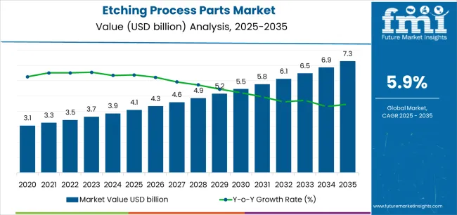
The etching process parts market benefits from technological transitions, including extreme ultraviolet lithography adoption requiring compatible etching processes, gate-all-around transistor architectures demanding precise vertical etching capabilities, and high aspect ratio features in 3D NAND memory necessitating selective etching chemistries and specialized chamber configurations. Rising complexity of semiconductor device architectures, increasing layer counts in memory devices exceeding 200 layers, and shrinking critical dimensions approaching atomic scale are compelling equipment manufacturers to invest in advanced etching process parts manufactured from high-purity materials with exceptional plasma resistance, thermal stability, and dimensional accuracy supporting the precision requirements of next-generation semiconductor fabrication processes across logic, memory, and specialty device categories.
The foundry and integrated device manufacturing (IDM) segment contributes significantly to market penetration, particularly in Asia-Pacific, where large-scale capacity expansions are underway. Major fabs in Taiwan, South Korea, Japan, and China are increasingly adopting high-durability silicon carbide and alumina parts that offer superior resistance to plasma erosion and thermal shock. The demand for etching process parts in these facilities is strongly linked to yield optimization and wafer throughput efficiency. In advanced foundries, performance differentiation is driven by the ability of chamber components to sustain millions of plasma cycles without particle generation or surface degradation. This reinforces the importance of precision machining, surface coating, and cleaning technologies within the global supply chain.
The equipment manufacturing sector also shows deep market penetration as OEMs refine chamber architectures to enhance plasma uniformity and etch selectivity. Manufacturers of dry etchers and plasma tools source specialized components from niche suppliers capable of maintaining nanometer-level tolerances. The adoption of etching process parts in this segment is being propelled by process modularization, where interchangeable part designs reduce downtime and improve tool maintenance efficiency.
In supporting industries, including microelectromechanical systems (MEMS), optoelectronics, and compound semiconductor manufacturing, demand is rising for tailored etching chamber components designed for high-aspect ratio structures and wide-bandgap materials such as GaN and SiC. These applications rely on etching process parts that can ensure precision plasma control and minimal defect generation during complex layer structuring.
Across all end-use sectors, performance differentiation is defined by three factors: material purity, erosion resistance, and thermal stability. As fabrication technology migrates toward more aggressive chemistries and higher aspect ratios, the adoption of etching process parts offering superior longevity, contamination control, and mechanical consistency continues to strengthen.
| Metric | Value |
|---|---|
| Market Value (2025) | USD 4.1 billion |
| Market Forecast Value (2035) | USD 7.3 billion |
| Forecast CAGR (2025-2035) | 5.9% |
| SEMICONDUCTOR INDUSTRY EXPANSION | TECHNOLOGY NODE ADVANCEMENT | EQUIPMENT & CAPACITY TRENDS |
|---|---|---|
|
|
|
| Category | Segments Covered |
|---|---|
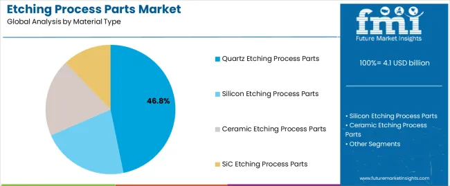
| By Material Type | Quartz Etching Process Parts, Silicon Etching Process Parts, Ceramic Etching Process Parts, SiC Etching Process Parts |
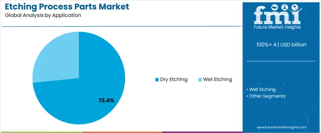
| By Application | Dry Etching, Wet Etching |
| By Region | North America, Europe, Asia Pacific, Latin America, Middle East & Africa |
| Segment | 2025 to 2035 Outlook |
|---|---|
| Quartz Etching Process Parts |
|
| Silicon Etching Process Parts |
|
| Ceramic Etching Process Parts |
|
| SiC Etching Process Parts |
|
| Segment | 2025 to 2035 Outlook |
|---|---|
| Dry Etching |
|
| Wet Etching |
|
| Region | Status & Outlook 2025-2035 |
|---|---|
| Asia Pacific |
|
| North America |
|
| Europe |
|
| DRIVERS | RESTRAINTS | KEY TRENDS |
|---|---|---|
|
|
|
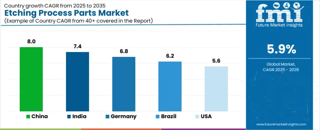
| Country | CAGR (2025-2035) |
|---|---|
| China | 8% |
| India | 7.4% |
| Germany | 6.8% |
| Brazil | 6.2% |
| USA | 5.6% |
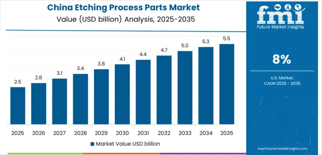
Revenue from etching process parts in China is projected to exhibit exceptional growth with a market value of USD 2.14 billion by 2035, driven by unprecedented semiconductor manufacturing capacity investments with government-supported development programs establishing comprehensive fabrication ecosystem and substantial funding supporting advanced node capability development. The country's ambition to achieve semiconductor self-sufficiency and ongoing fabrication facility construction across multiple regions creating massive equipment installations and corresponding parts requirements. Major foundries, memory manufacturers, and integrated device manufacturers including SMIC, YMTC, CXMT, and numerous emerging players establishing advanced manufacturing capabilities requiring extensive etching process equipment and consumable components.
Revenue from etching process parts in India is expanding to reach USD 1.77 billion by 2035, supported by government semiconductor manufacturing incentive programs including Production Linked Incentive schemes attracting substantial foreign investment and establishing fabrication capacity for diverse applications. The country's emerging position in global semiconductor supply chains with major international companies announcing manufacturing facilities and growing domestic design capabilities creating foundation for comprehensive ecosystem development. Strategic initiatives targeting semiconductor self-reliance and export-oriented manufacturing creating long-term growth trajectory.
Demand for etching process parts in Germany is projected to reach USD 1.53 billion by 2035, supported by the country's leadership in semiconductor equipment manufacturing with globally recognized companies producing etching systems and related process equipment establishing parts specifications and driving material innovations. German equipment manufacturers and materials suppliers maintaining technological advantages in high-purity materials and precision component fabrication. Domestic semiconductor manufacturing operations including specialized devices and research facilities creating local parts demand.
Revenue from etching process parts in Brazil is growing to reach USD 1.32 billion by 2035, driven by growing electronics manufacturing sector and emerging semiconductor industry development initiatives. Brazilian government and industry exploring semiconductor fabrication opportunities leveraging natural resources, technical workforce, and substantial domestic electronics consumption creating economic foundation for local manufacturing development. Regional positioning and trade relationships supporting potential role in Latin American semiconductor supply chains.
Demand for etching process parts in the USA is projected to reach USD 1.14 billion by 2035, driven by substantial fabrication capacity investments under CHIPS and Science Act supporting construction of multiple advanced semiconductor facilities by leading foundries and integrated device manufacturers. American semiconductor industry leadership in design, equipment manufacturing, and materials innovation driving technological advancement and establishing specifications for next-generation parts. Reshoring initiatives and supply chain security considerations supporting domestic manufacturing expansion.
Demand for etching process parts in the UK is projected to reach USD 983.9 million by 2035, supported by specialized semiconductor manufacturing strengths in compound semiconductors including gallium nitride and silicon carbide devices for power electronics and RF applications. British semiconductor industry characterized by design excellence, equipment innovation, and specialized device manufacturing requiring customized etching solutions. Government support for semiconductor industry development and research infrastructure supporting technology advancement.
Demand for etching process parts in Japan is projected to reach USD 869.3 million by 2035, driven by the country's leadership in semiconductor materials and equipment with globally dominant suppliers of high-purity quartz, silicon components, and advanced ceramics establishing quality standards and driving innovation. Japanese semiconductor manufacturing including leading-edge logic production by foundries and substantial memory manufacturing creating domestic parts demand. Equipment manufacturing capabilities with Japanese companies producing etching systems supporting ecosystem.
How Is the Etching Process Parts Market Distributed Across European Countries?
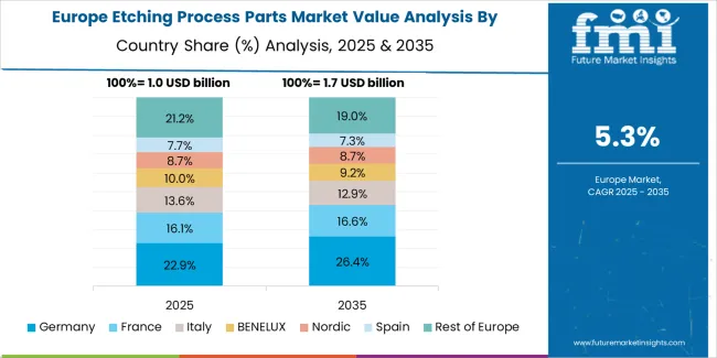
The etching process parts market in Europe is projected to grow from USD 406.9 million in 2025 to USD 719.8 million by 2035, registering a CAGR of 5.9% over the forecast period. Germany is expected to maintain its leadership position with a 32.4% market share in 2025, reaching 33.8% by 2035, supported by its semiconductor equipment manufacturing excellence, advanced materials expertise in high-purity quartz and technical ceramics, and growing fabrication investments under European Chips Act initiatives establishing new facilities.
France follows with a 16.8% share in 2025, projected to reach 17.3% by 2035, driven by specialized semiconductor device manufacturing, research and development infrastructure, and planned fabrication investments supporting European semiconductor ecosystem. The United Kingdom holds a 14.7% share in 2025, expected to stabilize at 15.2% by 2035, supported by compound semiconductor manufacturing strengths and specialized device production. Italy commands a 12.9% share, while Spain accounts for 10.8% in 2025, both benefiting from equipment manufacturing capabilities and growing electronics industry. The Rest of Europe region is anticipated to gain momentum, expanding its collective share from 12.4% to 12.7% by 2035, attributed to specialized semiconductor activities in Netherlands, Belgium, Austria, and other countries where research facilities, equipment manufacturing operations, and niche device production create parts demand supporting advanced technology development and European semiconductor supply chain strengthening initiatives.
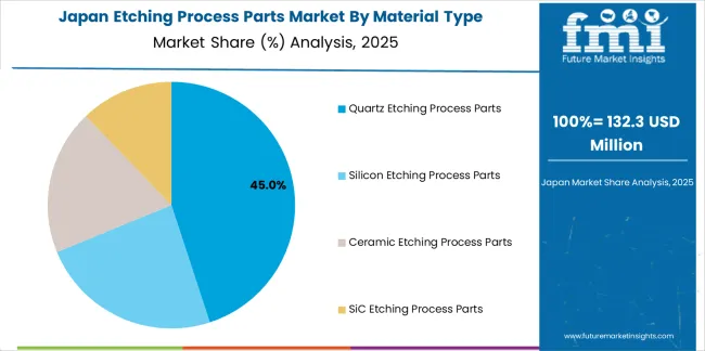
Japanese etching process parts operations reflect the country's global leadership in semiconductor materials manufacturing and exacting quality standards. Major materials suppliers including Tosoh Quartz Corporation, Shin-Etsu Chemical, and others maintain rigorous manufacturing processes ensuring exceptional purity levels, dimensional accuracy, and performance consistency that establish global benchmarks for etching chamber components. This dominance stems from decades of investment in high-purity materials expertise, advanced manufacturing capabilities, and close collaboration with equipment manufacturers and semiconductor fabs driving continuous improvement.
The Japanese market demonstrates unique strengths in materials science and precision manufacturing, with companies developing proprietary refining processes, advanced fabrication techniques, and comprehensive quality control systems achieving contamination levels measured in parts per billion. Equipment manufacturers worldwide rely on Japanese suppliers for critical high-purity quartz components where material quality directly impacts semiconductor yield and device reliability. Close integration between materials suppliers, equipment manufacturers, and semiconductor fabs enables rapid innovation cycles and performance optimization.
Regulatory oversight through Ministry of Economy, Trade and Industry supports semiconductor materials industry development while environmental regulations ensure sustainable manufacturing practices. Export control frameworks protect advanced materials technologies while enabling global market participation. Japanese companies' global market dominance reflects technical leadership rather than protective regulations, with performance advantages and established relationships creating natural competitive moats.
Supply chain management in Japanese semiconductor materials sector emphasizes long-term partnerships and continuous improvement through collaborative relationships. Materials suppliers work closely with equipment manufacturers through multi-year development programs optimizing component designs and material properties for next-generation etching systems. This approach supports substantial R&D investments and proprietary technology development while creating challenges for potential competitors lacking similar technical depth and customer relationships built over decades of performance excellence.
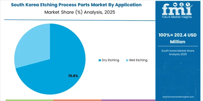
South Korean etching process parts operations reflect the country's position as global memory manufacturing leader with Samsung and SK Hynix operating advanced fabrication facilities consuming substantial quantities of etching equipment and replacement parts. Major semiconductor manufacturers drive demanding specifications for chamber components requiring exceptional quality and reliability supporting continuous high-volume production in leading-edge facilities. Korean memory manufacturing leadership creates substantial local parts demand while driving close relationships with global and domestic suppliers.
The Korean market demonstrates particular strength in high-volume manufacturing and rapid technology adoption, with memory manufacturers continuously advancing 3D NAND layer counts and DRAM scaling creating evolving parts requirements and driving material innovations. This creates opportunities for parts suppliers offering performance advantages, cost efficiencies, and responsive technical support. Growing Korean equipment manufacturing capabilities including specialized etching systems creating additional local market dynamics.
Regulatory frameworks through Ministry of Trade, Industry and Energy support semiconductor industry development through strategic initiatives while maintaining quality and safety standards. Government semiconductor investment programs and technology development support strengthening domestic ecosystem capabilities. Export controls on advanced materials and components reflecting strategic importance while enabling global market participation by Korean suppliers.
Supply chain efficiency remains critical given concentrated semiconductor manufacturing and just-in-time supply requirements minimizing inventory. Memory manufacturers maintain strategic supplier relationships ensuring reliable parts supply supporting continuous production while pursuing cost optimization and performance improvement. Growing domestic parts manufacturing capabilities with Korean companies developing quartz, silicon, and ceramic component production reducing import dependence and creating competitive alternatives to traditional suppliers while maintaining quality standards required for leading-edge manufacturing applications.
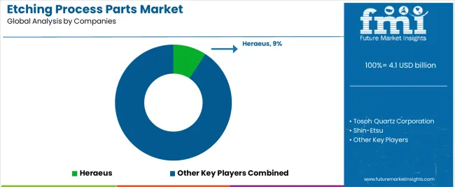
The etching process parts market exhibits concentrated leadership in high-purity materials segments with established Japanese, German, and American suppliers maintaining dominant positions through decades of materials science expertise, comprehensive quality systems, and established relationships with major equipment manufacturers. Market dynamics strongly favor incumbents with proven contamination control capabilities, established qualification status across multiple equipment platforms, and technical support infrastructure supporting global semiconductor manufacturing operations. Several distinct competitive archetypes define market structure: global materials science leaders offering comprehensive portfolios of high-purity quartz, silicon, and ceramic components with vertically integrated manufacturing and refining capabilities; specialized component manufacturers focusing on specific material categories or precision fabrication services; equipment manufacturer captive operations producing proprietary chamber components for internal use; and emerging regional suppliers particularly in China developing local manufacturing capabilities targeting cost-sensitive applications and reducing import dependence.
Competitive differentiation centers on material purity and consistency affecting semiconductor yield and contamination control, component dimensional accuracy and surface quality impacting process repeatability and particle generation, technical support capabilities including application engineering and process optimization consultation, and supply chain reliability ensuring on-time delivery supporting equipment manufacturing and fab operations. Qualification barriers remain substantial given extensive validation requirements for new suppliers, performance verification across multiple process conditions, and risk-averse procurement approaches in semiconductor industry where parts quality directly impacts multimillion-dollar wafer yields. Price competition intensifies in mature material categories and less demanding applications while premium segments maintain value-based pricing reflecting performance advantages and qualification investments.
Strategic imperatives include continuous materials innovation developing next-generation component solutions for emerging etching technologies, capacity expansion supporting growing semiconductor equipment demand and geographic diversification requirements, and qualification breadth expanding approved equipment platforms and customer relationships reducing concentration risks. Geographic strategy emphasizes proximity to major semiconductor manufacturing regions particularly Asia where concentrated fab capacity drives parts consumption while emerging markets including India present long-term growth opportunities. Technology development priorities include advanced coating technologies extending component lifetime and performance, additive manufacturing applications enabling complex geometries and customization, purity enhancement achieving lower contamination levels for leading-edge nodes, and alternative materials evaluation addressing supply risks and cost reduction opportunities while maintaining required performance characteristics.
| Items | Values |
|---|---|
| Quantitative Units | USD 4.1 billion |
| Material Type | Quartz Etching Process Parts, Silicon Etching Process Parts, Ceramic Etching Process Parts, SiC Etching Process Parts |
| Application | Dry Etching, Wet Etching |
| Regions Covered | North America, Latin America, Europe, Asia Pacific, Middle East & Africa |
| Country Covered | China, India, Germany, Brazil, United States, United Kingdom, Japan, South Korea, and other 35+ countries |
| Key Companies Profiled | Heraeus, Tosoh Quartz Corporation, Shin-Etsu, Schunk Xycarb Technology, MARUWA, CoorsTek, Ferrotec, Wonik QnC (Momentive), Worldex Industry, Kumkang Quartz Ltd, DS Techno Co., Ltd, Silfex Inc, Hana Materials Inc, Mitsubishi Materials, RS Technologies Co., Ltd, Tokai Carbon, Morgan Advanced Materials, AGC, SKC Solmics, SGL Carbon, Toyo Tanso, Mersen, SHINKONG, K Insulators, NTK CERATEC, TOTO, Sumitomo Osaka Cement, Entegris, MiCo, Kyocera, Technetics Group, Creative Technology Corporation, Krosaki Harima Corporation, AEGISCO, Coherent, Tsukuba Seiko, Hebei Sinopack Electronic, Shanghai QH Quartz, SICREAT (Suzhou) Semitech Co., Ltd, Coma Technology, One Semicon Co., Ltd, KC Parts Tech., Ltd., Thinkon Semiconductor, Techno Quartz Inc, Chongqing Zhenbao Technology Co., Ltd, Wuxi Rigetech, Huzhou Dongke Electronic Quartz Co, Hangzhou Hongxin Micro Semiconductor Co., Ltd, Shenyang Hanntek, Shanghai Ustron Quartz Glass Co., Ltd |
| Additional Attributes | Dollar sales by material type and application, regional demand (North America, Europe, Asia Pacific, Latin America, Middle East & Africa), competitive landscape, high-purity materials expertise, contamination control capabilities, and advanced manufacturing technologies driving performance enhancement, component lifetime extension, and semiconductor yield improvement |
The global etching process parts market is estimated to be valued at USD 4.1 billion in 2025.
The market size for the etching process parts market is projected to reach USD 7.3 billion by 2035.
The etching process parts market is expected to grow at a 5.9% CAGR between 2025 and 2035.
The key product types in etching process parts market are quartz etching process parts, silicon etching process parts, ceramic etching process parts and SiC etching process parts.
In terms of application, dry etching segment to command 73.4% share in the etching process parts market in 2025.
Full Research Suite comprises of:
Market outlook & trends analysis
Interviews & case studies
Strategic recommendations
Vendor profiles & capabilities analysis
5-year forecasts
8 regions and 60+ country-level data splits
Market segment data splits
12 months of continuous data updates
DELIVERED AS:
PDF EXCEL ONLINE
Dental Etching Liquid Market Size and Share Forecast Outlook 2025 to 2035
Tape Stretching Line Market Analysis – Growth & Trends 2025 to 2035
Electrolytic Etching Machine Market Size and Share Forecast Outlook 2025 to 2035
Raffia Tape Stretching Line Market
Process Automation and Instrumentation Market Size and Share Forecast Outlook 2025 to 2035
Process Pipe Coating Market Size and Share Forecast Outlook 2025 to 2035
Process Spectroscopy Market Analysis - Size, Share, and Forecast Outlook 2025 to 2035
Processed Beef Market Size and Share Forecast Outlook 2025 to 2035
Processed Fruit and Vegetable Market Analysis - Size, Share, and Forecast Outlook 2025 to 2035
Process Plants Gas Turbine Market Analysis - Size, Share, and Forecast Outlook 2025 to 2035
Competitive Breakdown of Processed Beef Market Share
Market Share Insights for Processed Cashew Providers
Analysis and Growth Projections for Processed Superfruit Market
Processed Meat Market Analysis by Type, Packaging, Meat Type, and Region through 2035
Process Liquid Analyzer Market Growth - Trends & Forecast 2025 to 2035
Process Instrumentation Market Growth - Trends & Forecast 2025 to 2035
Analysis and Growth Projections for Processed Cheese Market
Evaluating Process Automation and Instrumentation Market Share & Provider Insights
Processed Cashew Market Trends – Snack Innovation & Industry Growth 2025 to 2035
Processed Meat Packaging Market Growth & Trends 2024 to 2034

Thank you!
You will receive an email from our Business Development Manager. Please be sure to check your SPAM/JUNK folder too.
Chat With
MaRIA