- Market Size (2026)
- USD 6.1 Bn
- Forecast (2036)
- USD 20.9 Bn
- CAGR (2026 to 2036)
- 13.1%
How big is Atomic Layer Etch Equipment Market in 2026?
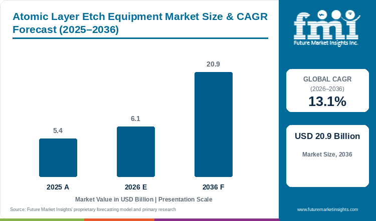
Demand for atomic layer etch equipment is projected to expand at 13.1% CAGR between 2026 and 2036. Industry value grows from USD 5.4 billion in 2025 to USD 6.1 billion in 2026 and is projected to reach USD 20.9 billion by 2036.
Sales of atomic layer etch equipment are rising at a steady pace due its ability to remove very thin material from semiconductor wafers through repeated activation and removal steps. The global atomic layer etch equipment market was valued at USD 5.4 billion in 2025 and is projected to grow from USD 6.1 billion in 2026 to USD 20.9 billion by 2036, at 13.1% CAGR. As per FMI, 300 mm advanced-fab wafers will hold 34.8% of wafer size compatibility demand in 2026. SEMI projected USD 143.9 billion of wafer fab equipment sales in 2026.[1] Lam Research reported an installed base of more than 30,000 Kiyo etch chambers across global manufacturing lines.[2] Applied Materials also introduced Producer Selectra Mo Etch in June 2026 for selective molybdenum removal in 3D NAND.[3] Expansion of three-dimensional logic and memory production is expected to drive atomic layer etch equipment demand.
Key Market Trends & Insights
- By wafer size compatibility, 300 mm advanced-fab wafers led with 34.8% share in 2026, supported by high-volume logic and memory production.
- By process node, leading-edge sub-5 nm nodes accounted for 40.1% in 2026, aligned with gate-all-around and advanced memory etch requirements.
- By system architecture, automated vacuum cluster tools represented 45.3% in 2026, owing to connected activation, removal and wafer-handling operations.
- By end user tier, integrated device manufacturers held 36.6% in 2026, as device design and production qualification are managed within the same fab network.
Regional Highlights
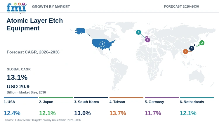
- Fastest-growing profiled country: Taiwan (13.7% CAGR, 2026 to 2036).
- By country: South Korea (13.0%) and the USA (12.4%) follow, while Germany records the lowest profiled CAGR at 11.7%.
Market Size & Forecast
Table 1: Market Size and Forecast for the Atomic Layer Etch Equipment Market (USD billion and percentage), 2025 to 2036
| Metric | Value |
|---|---|
| 2025 Market Size | USD 5.4 billion |
| Estimated Market Size in 2026 | USD 6.1 billion |
| Projected Market Size by 2036 | USD 20.9 billion |
| CAGR, 2026 to 2036 | 13.1% |
| Added Revenue, 2026 to 2036 | USD 14.8 billion |
| Market Expansion Multiple | 3.4x |
New wafer fabs require etch tools alongside broader wafer processing equipment before starting qualified semiconductor production. TSMC announced planned United States investment of USD 165 billion in March 2025, covering three new fabs, two advanced packaging facilities and one research center.[4] In November 2025, Oxford Instruments supplied automated 6-inch InP equipment which provides more than four times devices per wafer and supports movement from 800G to 1.6T products.[5] KLA reported about 11% growth in fiscal 2025 specialty semiconductor process revenue and 25% growth in process-control revenue.[6] These developments indicate that fab construction, larger wafer processing and process inspection will support equipment installations over the forecast period.
Fabrication Capacity and Etch Demand Indicators
Atomic layer etch equipment forms a part of the complete wafer processing line. Semiconductor manufacturers install these systems when thin materials cannot be removed through continuous etching without affecting nearby layers. Fab spending indicates the volume of semiconductor manufacturing equipment that can be installed, while chamber base and wafer output show whether the process can support commercial production. These indicators connect semiconductor manufacturing activity with future atomic layer etch equipment demand.
Table 2: Fabrication Capacity and Etch Demand Indicators for the Atomic Layer Etch Equipment Market (USD billion, chambers, percentages, and wafer productivity), mixed reporting years from 2025 to 2026
| Indicator | Data Point | Why It Matters | Source |
|---|---|---|---|
| 2026 wafer fab equipment sales forecast | USD 143.9 billion | Shows spending available for wafer processing, facilities and related fab equipment. | [1] |
| Lam Kiyo installed production base | More than 30,000 chambers | Provides a production reference for migration toward newer conductor etch platforms. | [2] |
| Akara plasma response | 100 times faster | Connects faster plasma control with narrow three-dimensional logic and memory structures. | [8] |
| Automated 6-inch InP processing | More than four times devices per wafer | Shows how larger automated wafers can increase output for photonic semiconductor production. | [5] |
| KLA specialty semiconductor process growth | About 11% in fiscal 2025 | Indicates current growth in deposition and etch process tools serving specialty applications. | [6] |
Basis: Supporting indicators use mixed reporting years and do not represent atomic layer etch equipment market share.
Analyst Perspective
“I expect fabs to favour atomic layer etch systems which holds profile control without reducing production wafer output. Wider adoption will follow when chamber matching and particle performance remains stable across continuous high-volume production.”
- Nikhil Kaitwade, Principal Consultant, Future Market Insights.
How is the atomic layer etch equipment market segmented?
Atomic layer etch equipment market is segmented by four primary commercial axes and region: wafer size compatibility, process node, system architecture, end user tier, and region. In 2026, 300 mm advanced-fab wafers are estimated at 34.8%, sub-5 nm nodes at 40.1%, automated vacuum cluster tools at 45.3%, and integrated device manufacturers at 36.6%.
By wafer size compatibility: 300 mm advanced-fab wafers, 200 mm legacy-fab wafers, and compound semiconductor substrates.
By process node: leading-edge sub-5 nm nodes, mature 7 nm to 28 nm nodes, and legacy power and discrete nodes.
By system architecture: automated vacuum cluster tools, in-line track systems, single-wafer processing chambers, and batch immersion modules.
By end user tier: integrated device manufacturers, pure-play foundries, outsourced semiconductor assembly and test providers, and advanced research cleanrooms.
By region: North America, Latin America, Western Europe, Eastern Europe, East Asia, South Asia and Pacific, and Middle East and Africa.
Why do 300 mm wafers retain a notable equipment share?
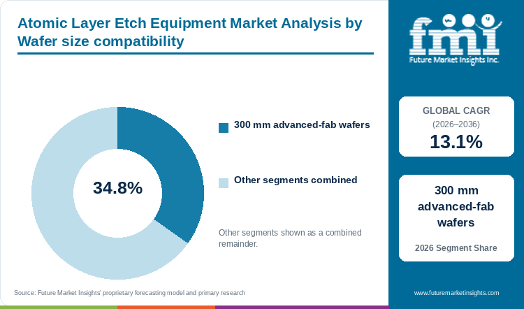
300 mm advanced-fab wafers are projected to capture 34.8% of wafer size compatibility revenue in 2026, supported by high-volume fab standardization.
Table 3: Wafer Size Compatibility Share for the Atomic Layer Etch Equipment Market (percentage share), 2026
| Wafer Size Compatibility | Share (2026) |
|---|---|
| 300 mm Advanced-Fab Wafers | 34.8% |
| Other Segments Combined | 65.2%* |
| Total | 100.0% |
*Calculated as the balance remaining after deducting the leading segment’s reported share from 100.0%.
Table 4: Wafer Size Compatibility Leadership and Market Growth for the Atomic Layer Etch Equipment Market (segment and CAGR percentage), 2026 to 2036
| Metric | Value |
|---|---|
| Global CAGR (2026 to 2036) | 13.1% |
| Leading Segment | 300 mm Advanced-Fab Wafers |
| Leading Segment Share (2026) | 34.8% |
300 mm advanced-fab wafers are widely used in high-volume logic and memory production. A larger wafer provides more dies in one cycle, due to which manufacturers install advanced etch modules on 300 mm production lines. In the FMI report, the segment accounts for 34.8% of wafer size compatibility revenue in 2026. Availability of new 300 mm capacity is anticipated to support demand for chamber matching and connected wafer manufacturing equipment.
- 300 mm advanced-fab wafers account for 34.8% share in 2026, supported by high-volume logic and memory fabs standardizing advanced process modules.
- In April 2026, SEMI projected global 300mm front-end fab equipment spending to reach a record USD 149 billion, representing double-digit annual growth driven by logic and memory expansion.[7]
What supports sub-5 nm nodes as a preferred process category?
Leading-edge sub-5 nm nodes are estimated to represent 40.1% of process node revenue in 2026, reflecting narrow gate-all-around profile requirements.
Leading-edge sub-5 nm nodes require removal of thin materials from narrow semiconductor structures. Atomic layer etching removes material in repeated steps and protects the nearby layer from excessive plasma exposure. Combined with atomic layer deposition for conformal film growth, atomic layer etching enables angstrom-scale structural control across 3D devices. Sub-5 nm nodes are estimated to hold 40.1% of process node revenue in 2026. Wider production of three-dimensional devices is expected to support the segment growth during the forecast period.
- Leading-edge sub-5 nm nodes account for 40.1% share in 2026, reflecting gate-all-around structures requiring narrow process windows and controlled profile transfer.
- In February 2025, Lam Research described Akara conductor etch control as responding to plasma changes 100 times faster than existing sources.[8]
How do cluster tools meet changing fab integration needs?
Automated vacuum cluster tools are anticipated to contribute 45.3% of system architecture revenue in 2026, owing to connected multi-chamber vacuum processing.
Automated vacuum cluster tools combine etching with wafer cleaning equipment and transport chambers under one connected production system. The wafer remains under controlled vacuum between process steps, due to which surface exposure and additional handling is reduced. FMI data suggests that automated vacuum cluster tools will account for 45.3% of system architecture revenue in 2026. Lam Research includes atomic layer etching under its Flex dielectric etch family for memory, packaging, patterning and transistor applications. These factors are likely to drive demand for automated vacuum cluster tools.
- Automated vacuum cluster tools account for 45.3% share in 2026, owing to linked chambers that reduce wafer exposure between activation and removal steps.
- Lam Research lists atomic layer etching within its Flex dielectric etch family for advanced memory, packaging, patterning, and transistor applications.[9]
Why do integrated manufacturers anchor end-user equipment demand?
Integrated device manufacturers are set to command 36.6% of end user tier revenue in 2026, reinforced by internal fab qualification.
Integrated device manufacturers develop semiconductor designs and also operate wafer production facilities. This allows atomic layer etch systems to be checked alongside specialized 3D NAND metrology equipment before installing more production chambers. According to FMI, integrated device manufacturers will hold 36.6% of end user tier revenue in 2026. Direct ownership of device and process development is expected to support equipment adoption among integrated manufacturers.
- Integrated device manufacturers account for 36.6% share in 2026, underpinned by device ownership connecting process development directly with production qualification.
- In commercial memory production, integrated device manufacturers such as Samsung implemented multi-step atomic layer etching across high-aspect-ratio 3D NAND and DRAM fabrication lines.[10]
What are the drivers, restraints, and opportunities in the atomic layer etch equipment market?
In the atomic layer etch equipment market, advanced device scaling is the key driver, process throughput is the key restraint, and fab expansion is the key opportunity.
- Driver: Gate-all-around logic, three-dimensional memory, and narrow interconnects expand demand for controlled material removal.
- Restraint: Multi-step cycling, particles, and chamber complexity can lower throughput and delay production qualification.
- Opportunity: New advanced fabs create openings for integrated etch platforms, process modules, and local service capacity.
Device Scaling Increases Etch Precision
Gate-all-around logic and three-dimensional memory contain narrow structures where nearby materials have to remain protected during etching. Fabs rely on specialized ALD precursors and self-limiting reactions to form and clear alternating layers without distorting adjacent features. A 2025 technical review in Nanoscale Advances stated that atomic layer etching supports high-aspect-ratio structures through layer-by-layer removal.[11] Lower surface damage allows manufacturers to maintain the required profile during critical etch steps. These properties are expected to drive atomic layer etch equipment market growth as advanced semiconductor production expands.
Cycle Throughput Restricts Wider Use
Atomic layer etching uses separate activation and removal steps, due to which the process takes longer than continuous plasma etching. A 2026 industrial review in the International Journal of Extreme Manufacturing identified low throughput, particles, imperfect self-limiting reaction and process complexity as adoption barriers.[12] Higher cycle time can lower wafer output and accelerates wear on consumable parts for semiconductor equipment across multi-chamber platforms. These issues may hamper wider use of atomic layer etch equipment in high-volume semiconductor fabs.
Fab Programs Expand Qualification Openings
New semiconductor fabs are creating opportunities for atomic layer etch equipment manufacturers. In February 2025, the German Federal Ministry for Economic Affairs and Climate Action approved support under the European Chips Act for a new 300 mm frontend production module in Dresden, involving about USD 3.6 billion equivalent in total investment.[13] Such fabs require etch platforms, chemical vapor deposition systems, and local service before commercial wafer production starts. Growing number of new wafer lines is expected to create growth opportunities during the assessment period.
Which country CAGRs are profiled in the atomic layer etch equipment market?
Table 5: Country CAGR Comparison for the Atomic Layer Etch Equipment Market (CAGR percentage), 2026 to 2036
| Country | CAGR |
|---|---|
| USA | 12.4% |
| Japan | 12.1% |
| South Korea | 13.0% |
| Taiwan | 13.7% |
| Germany | 11.7% |
| Netherlands | 12.1% |
How do country-level CAGRs compare in the atomic layer etch equipment market?
East Asia atomic layer etch equipment demand is expected to grow owing to expansion of foundry and advanced memory production. Taiwan is projected at 13.7% CAGR through 2036, while South Korea follows at 13.0% owing to larger memory manufacturing base. The USA at 12.4% and Japan at 12.1% will develop through new fabs and next-generation logic programs. Germany and the Netherlands are projected at 11.7% and 12.1%, respectively, supported by European production and equipment technologies.
As per the analysis from FMI, Taiwan and South Korea will record higher growth as foundry and memory manufacturers add advanced production capacity. The USA and Japan are increasing domestic semiconductor manufacturing, whereas Germany and the Netherlands are developing through new wafer lines and equipment research.
- USA demand is tied to new domestic fabs, tool installation, and production ramp schedules.
- Japan connects next-generation logic funding with established materials and equipment suppliers.
- South Korea gains from advanced memory structures that require deep and selective etch steps.
- Taiwan combines large equipment budgets with dense foundry and packaging capacity.
- Germany adds 300 mm capacity in Dresden for power, analog, and mixed-signal devices.
- Netherlands demand is influenced by equipment innovation and expanded export authorization requirements.
Full report country CAGRs cover: North America; Latin America; Western Europe; Eastern Europe; East Asia; South Asia and Pacific; Middle East and Africa.
Country-wise Analysis
- By 2036, the USA is projected to grow at 12.4% CAGR, supported by federal manufacturing incentives and commercial fab construction. In January 2025, the U.S. Department of Commerce finalized major CHIPS and Science Act awards, directing over USD 33 billion in incentives across commercial fabrication facilities and advanced wafer lines.[14] These production sites require etch, deposition, cleaning and inspection equipment before starting volume output. Installation schedules and process qualification will influence how quickly the investment creates equipment orders.
- Japan atomic layer etch equipment market is anticipated to advance at 12.1% CAGR over the assessment period. In November 2025, METI selected Rapidus for financial support through the fiscal 2025 budget.[15] Rapidus is developing a 2 nm production route where gate-all-around structures require narrow profile transfer and lower wafer damage. Japan also has established semiconductor materials, equipment and metrology manufacturers. Movement from pilot production towards commercial wafer output is anticipated to support equipment demand in Japan.
- Advanced memory production is expected to raise atomic layer etch equipment demand in South Korea at 13.0% CAGR through 2036. South Korean fabs produce DRAM, NAND and high-bandwidth memory where deeper structures require selective etching. In December 2025, the Ministry of Trade, Industry and Energy announced expanded capital support to accelerate high-bandwidth memory fab clusters.[16] Growing memory layer count is expected to drive equipment demand over the forecast period.
- Taiwan atomic layer etch equipment market is estimated to expand at 13.7% CAGR through 2036, supported by foundry and packaging investment. In September 2025, the Chip-based Industrial Innovation Office reported that Taiwan expected USD 27.9 billion of semiconductor equipment spending in 2025, nearly 70% above 2024.[17] The same source placed South Korea at USD 24.9 billion for the year. Taiwan has a large foundry base where etch tools are tested with lithography, deposition and metrology systems. Presence of suppliers and field support is expected to propel the market growth.
- The Germany atomic layer etch equipment sector is projected to record 11.7% CAGR during the assessment period, supported by cleanroom expansions in Silicon Saxony. The German Federal Office for Economic Affairs and Export Control recorded expanded microelectronics manufacturing investments across Silicon Saxony for 300 mm power and mixed-signal capacity.[18] Expansion of this production line is likely to support demand for etch systems having longer chamber life and flexible recipes.
- Atomic layer etch equipment demand in the Netherlands is predicted to advance at 12.1% CAGR through 2036. From April 1, 2025, the government expanded authorization requirements to selected measuring and inspection technologies used in advanced semiconductor manufacturing.[19] Export applications are reviewed separately for destinations outside the European Union. The measure is not an export ban, but it can change the timing of equipment shipment. Equipment research and nearby European fabs are expected to support demand during the forecast period.
Who are the notable companies in the atomic layer etch equipment market?
Lam Research, Applied Materials, Tokyo Electron, Hitachi High-Tech, Oxford Instruments, Plasma-Therm, SCREEN Holdings, and KLA Corporation are notable companies profiled in this market.
Atomic layer etch equipment market is concentrated among semiconductor process equipment companies and specialized plasma system suppliers. Lam Research, Applied Materials and Tokyo Electron offer etch equipment for high-volume logic and memory fabs. Oxford Instruments and Plasma-Therm are focusing on compound semiconductor, photonics and research applications. KLA, Hitachi High-Tech and SCREEN Holdings participate through process control, metrology, cleaning and related wafer equipment. Some of the key players are expanding product capability and local services in order to cater to the growing production requirement.
- High-volume etch platforms: Lam Research, Applied Materials, and Tokyo Electron.
- Research and specialty etch systems: Oxford Instruments and Plasma-Therm.
- Process control and integration participants: KLA Corporation, Hitachi High-Tech, and SCREEN Holdings.
Competitive Benchmarking: Atomic Layer Etch Equipment Market
Table 6: Competitive Benchmarking for the Atomic Layer Etch Equipment Market (qualitative capability ratings), 2026
| Company | ALE Depth | Integration | Current Activity | Reach |
|---|---|---|---|---|
| Lam Research | High | High | High | High |
| Applied Materials | High | High | High | High |
| Tokyo Electron | High | High | High | High |
| Hitachi High-Tech | Medium | Medium | Medium | High |
| Oxford Instruments | High | Medium | Medium | High |
| Plasma-Therm | Medium | Medium | Medium | Medium |
| SCREEN Holdings | Medium | High | Medium | High |
| KLA Corporation | Medium | High | High | High |
High indicates broad public evidence across product depth, integration, current activity, or geographic reach. Medium indicates narrower public evidence. Low would indicate limited direct evidence. Ratings do not represent product quality, market share, or company rank.
Key Developments in the Atomic Layer Etch Equipment Market
- In February 2026, Applied Materials introduced the Sym3 Z Magnum conductor etch system with fine-pitch feature profile control for 2 nm gate-all-around nodes.[20]
- In September 2025, Lam Research and JSR/Inpria entered a cross-licensing and collaboration agreement covering materials for advanced atomic layer deposition and etch solutions.[21]
- In September 2025, Taiwan’s Ministry of Economic Affairs presented 37 semiconductor technologies covering AI chips, advanced manufacturing, testing equipment, and compound semiconductors.[22]
- In March 2026, Plasma-Therm announced sustained demand for its CHA Mark Series tool platform, supporting precision thin-film and specialty etch applications.[23]
Key Players in the Atomic Layer Etch Equipment Market
High-volume Process Equipment Platforms
- Lam Research
- Applied Materials
- Tokyo Electron
Specialty and Research Etch Platforms
- Oxford Instruments
- Plasma-Therm
Process Control and Integration Participants
- Hitachi High-Tech
- SCREEN Holdings
- KLA Corporation
Atomic Layer Etch Equipment Market - Report Scope
Table 7: Report Scope for the Atomic Layer Etch Equipment Market (coverage fields and definitions), 2026 to 2036
| Coverage field | Report scope |
|---|---|
| Market breakdown | Wafer size compatibility; process node; system architecture; end user tier; region |
| Quantitative units | USD billion |
| Market definition | First-sale revenue from systems and directly integrated modules used for cyclic, layer-controlled semiconductor material removal. Standalone consumables and unrelated plasma tools are excluded. |
| Regions covered | North America; Latin America; Western Europe; Eastern Europe; East Asia; South Asia and Pacific; Middle East and Africa |
| Countries covered | USA; Japan; South Korea; Taiwan; Germany; Netherlands |
| Key companies profiled | Lam Research; Applied Materials; Tokyo Electron; Hitachi High-Tech; Oxford Instruments; Plasma-Therm; SCREEN Holdings; KLA Corporation |
| Forecast period | 2026 to 2036 |
| Approach | Hybrid bottom-up and top-down sizing based on fab investment, etch steps, tool qualification, installed base, and country demand conditions. |
Atomic Layer Etch Equipment Market - Research Methodology
Table 8: Research Methodology for the Atomic Layer Etch Equipment Market (research methods and approach), 2026 edition
| Method | Approach |
|---|---|
| Primary Research | The research study includes interviews with equipment manufacturers, service providers, technology developers, end users, procurement teams and industry experts. Interviews covers equipment selection, pricing, adoption barriers, approval requirement and technical support. |
| Desk Research | Desk research includes government publications, regulatory records, technical literature, company filings, product information and official announcements. Sources are reviewed for publication date, market relevance and consistency with the defined equipment scope. |
| Market Sizing and Forecasting | Market sizing combines the baseline value with equipment pricing, installed chambers, fab investment, segment structure and country demand conditions. Forecast assumptions considers technology adoption, purchasing cycles, supply availability and barriers affecting wider production use. |
| Data Validation | Market estimates are checked with public data, company activity, technical evidence and findings from primary interviews. Adjacent tools, unsupported claims and overlapping revenue are excluded from final calculations. |
Atomic Layer Etch Equipment Market by Segments
Atomic layer etch equipment market segmented by Wafer size compatibility:
- 300 mm advanced-fab wafers
- 200 mm legacy-fab wafers
- Compound semiconductor substrates
Atomic layer etch equipment market segmented by Process node:
- Leading-edge sub-5 nm nodes
- Mature 7 nm to 28 nm nodes
- Legacy power and discrete nodes
Atomic layer etch equipment market segmented by System architecture:
- Automated vacuum cluster tools
- In-line track systems
- Single-wafer processing chambers
- Batch immersion modules
Atomic layer etch equipment market segmented by End user tier:
- Integrated device manufacturers
- Pure-play foundries
- Outsourced semiconductor assembly and test providers
- Advanced research cleanrooms
Atomic Layer Etch Equipment Market by Region
- North America
- United States
- Canada
- Latin America
- Brazil
- Mexico
- Argentina
- Chile
- Western Europe
- Germany
- France
- United Kingdom
- Italy
- Spain
- Benelux
- Nordics
- Eastern Europe
- Poland
- Czech Republic
- Romania
- Hungary
- East Asia
- Japan
- South Korea
- Taiwan
- South Asia and Pacific
- ASEAN
- Australia and New Zealand
- Middle East and Africa
- GCC Countries
- South Africa
- Türkiye
- Israel
Research Sources and Bibliography
- [1] SEMI. (2026, July 14). Global semiconductor equipment sales forecast to reach a record USD 229 billion in 2028, SEMI reports.
- [2] Lam Research Corporation. (2026). Etch products: Creating features with atomic precision.
- [3] Applied Materials, Inc. (2026, June 15). Applied Materials unveils deposition and selective etch systems to advance 3D chip scaling.
- [4] Taiwan Semiconductor Manufacturing Company Limited. (2025, March 4). TSMC intends to expand its investment in the United States to US$165 billion to power the future of AI.
- [5] Oxford Instruments plc. (2025, November 17). Enabling AI with fully automated equipment for 6-inch InP wafer processing.
- [6] KLA Corporation. (2025). 2025 letter to stockholders.
- [7] SEMI. (2026, April 1). SEMI projects double-digit growth in global 300mm fab equipment spending for 2026 and 2027.
- [8] Lam Research Corporation. (2025, February 19). Akara: A generational leap in semiconductor etch with unmatched precision.
- [9] Lam Research Corporation. (2026). Flex dielectric etch systems: Precision profile control for advanced semiconductor manufacturing.
- [10] Lee, S., Ra, H., & Bai, K. H. (2026, August 25). Current status of atomic layer etching and its adoption to low-k fine patterning: An industrial perspective. Journal of Vacuum Science & Technology A, 44, 058501.
- [11] Lee, T.-Y., Chen, P.-T., Huang, C.-C., et al. (2025, April 11). Advances in core technologies for semiconductor manufacturing. Nanoscale Advances, 7, 2796-2817.
- [12] International Journal of Extreme Manufacturing. (2026, March 23). Atomic layer etching for extreme manufacturing: Pushing the limits of atomic scale precision.
- [13] Federal Ministry for Economic Affairs and Climate Action. (2025, February 20). European Commission approves another German Chips Act project: Infineon expands chip production in Dresden.
- [14] U.S. Department of Commerce. (2025, January 17). U.S. Department of Commerce announces CHIPS incentives awards to support commercial fabrication facilities.
- [15] Ministry of Economy, Trade and Industry. (2025, November 21). Press conference by Minister Akazawa: Next-generation semiconductor manufacturer selected for financial support.
- [16] Ministry of Trade, Industry and Energy. (2025, December 29). Comprehensive measures to strengthen the competitiveness of the advanced semiconductor ecosystem.
- [17] Chip-based Industrial Innovation Office. (2025, September 8). SEMICON Taiwan 2025 launches with record 56 countries and 100,000 visitors anticipated.
- [18] Federal Ministry for Economic Affairs and Climate Action. (2025, May 15). Microelectronics in Germany: Silicon Saxony manufacturing and investment report.
- [19] Government of the Netherlands. (2025, January 15). Export controls on advanced semiconductor manufacturing equipment to be tightened.
- [20] Applied Materials, Inc. (2026, February 10). Applied Materials unveils transistor and wiring innovations for faster AI chips.
- [21] Lam Research Corporation & JSR Corporation. (2025, September 15). Cross-licensing and collaboration agreement to advance semiconductor manufacturing.
- [22] Ministry of Economic Affairs, R.O.C. (2025, September 12). MOEA showcases silicon photonics and 3D chip modules to strengthen Taiwan semiconductor innovation chain.
- [23] Plasma-Therm LLC. (2026, March 18). CHA Mark Series upgrade highlights continued demand.
This bibliography is provided for reader reference. The full report contains the complete reference list and detailed citations.
This Report Answers
- How large is the atomic layer etch equipment market in 2026?
- What market value is projected for atomic layer etch equipment by 2036?
- Which wafer size holds a notable equipment share in 2026?
- Which process node represents a notable equipment share in 2026?
- Which country has a notable expansion outlook through 2036?
- Which companies are notable in the atomic layer etch equipment market?
Frequently Asked Questions
How large is the atomic layer etch equipment market in 2026?
Future Market Insights estimates that atomic layer etch equipment market will be valued at USD 6.1 billion in 2026. The market is projected to reach USD 20.9 billion by 2036.
What CAGR is projected for atomic layer etch equipment through 2036?
FMI research indicates, atomic layer etch equipment market is projected to grow at 13.1% CAGR from 2026 to 2036. Growth is supported by advanced logic and memory devices requiring controlled material removal.
Which wafer size holds notable market share in 2026?
300 mm advanced-fab wafers are projected to hold 34.8% of wafer size compatibility revenue in 2026. The segment benefits from high-volume logic and memory production using integrated process tools.
Which process node holds a notable share in 2026?
Leading-edge sub-5 nm nodes are estimated to account for 40.1% of process node revenue in 2026. Demand is supported by gate-all-around structures and narrow semiconductor process windows.
Which country has notable expansion outlook through 2036?
Taiwan is projected to register 13.7% CAGR from 2026 to 2036. Foundry capacity, advanced packaging and semiconductor equipment investment supports the country growth outlook.
Who are the key companies in atomic layer etch equipment market?
Key companies include Lam Research, Applied Materials, Tokyo Electron, Hitachi High-Tech, Oxford Instruments, Plasma-Therm, SCREEN Holdings, and KLA Corporation. These companies are focusing on etch precision, process integration and technical support near semiconductor fabs.
Preview the report firsthand - request a free sample
Get SampleGet the brochure for pricing and purchase details.
Get PDFTable of Content
- Key Takeaways
- Market Size and CAGR
- Top Growth Driver
- Fastest Growing Segment
- Leading Region
- Key Companies
- Emerging Opportunities
- Executive Summary
- Global Market Outlook
- Demand-side Trends
- Supply-side Trends
- Technology Roadmap Analysis
- Analysis and Recommendations
- Analyst Perspective (What is happening? Why now? What should investors know?)
- Key Questions Answered
- How large is the market?
- What is the CAGR?
- What are key trends?
- Which region dominates?
- Who are the leaders?
- Market Overview
- Market Coverage / Taxonomy
- Market Definition / Scope / Limitations
- Research Methodology
- Chapter Orientation
- Analytical Lens and Working Hypotheses
- Market Structure, Signals, and Trend Drivers
- Benchmarking and Cross-market Comparability
- Market Sizing, Forecasting, and Opportunity Mapping
- Research Design and Evidence Framework
- Desk Research Programme (Secondary Evidence)
- Expert Input and Fieldwork (Primary Evidence)
- Tooling, Models, and Reference Databases
- Data Engineering and Model Build
- Quality Assurance and Audit Trail
- Market Background
- Market Dynamics (Drivers, Restraints, Opportunity, Trends)
- Scenario Forecast (Optimistic, Likely, Conservative)
- Impact Analysis
- AI Impact
- Sustainability Impact
- Regulatory Impact
- Technology Impact
- Consumer / Buyer Analysis
- Purchase Drivers
- Adoption Barriers
- Buyer Journey
- Opportunity Map Analysis
- Product Life Cycle Analysis
- Supply Chain Analysis
- Investment Feasibility Matrix
- Value Chain Analysis
- PESTLE and Porter's Analysis
- Regulatory Landscape
- Regional Parent Market Outlook
- Production and Consumption Statistics
- Import and Export Statistics
- Global Market Analysis and Forecast, 2021 to 2036
- Historical Market Size Value (USD Billion) Analysis, 2021 to 2025
- Current and Future Market Size Value (USD Billion) Projections, 2026 to 2036
- Y-o-Y Growth Trend Analysis
- Absolute $ Opportunity Analysis
- Global Market Pricing Analysis, 2021 to 2036
- Global Market Analysis and Forecast, By Wafer size compatibility, 2021 to 2036
- Introduction / Key Findings
- Historical Market Size Value (USD Billion) Analysis By Wafer size compatibility, 2021 to 2025
- Current and Future Market Size Value (USD Billion) Analysis and Forecast By Wafer size compatibility, 2026 to 2036
- 300 mm advanced-fab wafers
- 200 mm legacy-fab wafers
- Compound semiconductor substrates
- Y-o-Y Growth Trend Analysis By Wafer size compatibility, 2021 to 2025
- Absolute $ Opportunity Analysis By Wafer size compatibility, 2026 to 2036
- Global Market Analysis and Forecast, By Process node, 2021 to 2036
- Introduction / Key Findings
- Historical Market Size Value (USD Billion) Analysis By Process node, 2021 to 2025
- Current and Future Market Size Value (USD Billion) Analysis and Forecast By Process node, 2026 to 2036
- Leading-edge sub-5 nm nodes
- Mature 7 nm to 28 nm nodes
- Legacy power and discrete nodes
- Y-o-Y Growth Trend Analysis By Process node, 2021 to 2025
- Absolute $ Opportunity Analysis By Process node, 2026 to 2036
- Global Market Analysis and Forecast, By System architecture, 2021 to 2036
- Introduction / Key Findings
- Historical Market Size Value (USD Billion) Analysis By System architecture, 2021 to 2025
- Current and Future Market Size Value (USD Billion) Analysis and Forecast By System architecture, 2026 to 2036
- Automated vacuum cluster tools
- In-line track systems
- Single-wafer processing chambers
- Batch immersion modules
- Y-o-Y Growth Trend Analysis By System architecture, 2021 to 2025
- Absolute $ Opportunity Analysis By System architecture, 2026 to 2036
- Global Market Analysis and Forecast, By End user tier, 2021 to 2036
- Introduction / Key Findings
- Historical Market Size Value (USD Billion) Analysis By End user tier, 2021 to 2025
- Current and Future Market Size Value (USD Billion) Analysis and Forecast By End user tier, 2026 to 2036
- Integrated device manufacturers
- Pure-play foundries
- Outsourced semiconductor assembly and test providers
- Advanced research cleanrooms
- Y-o-Y Growth Trend Analysis By End user tier, 2021 to 2025
- Absolute $ Opportunity Analysis By End user tier, 2026 to 2036
- Global Market Analysis and Forecast, By Region, 2021 to 2036
- Introduction
- Historical Market Size Value (USD Billion) Analysis By Region, 2021 to 2025
- Current Market Size Value (USD Billion) Analysis and Forecast By Region, 2026 to 2036
- North America
- Latin America
- Western Europe
- Eastern Europe
- East Asia
- South Asia and Pacific
- Middle East and Africa
- Market Attractiveness Analysis By Region
- North America Market Analysis and Forecast, By Country, 2021 to 2036
- Historical Market Size Value (USD Billion) Trend Analysis By Market Taxonomy, 2021 to 2025
- Market Size Value (USD Billion) Forecast By Market Taxonomy, 2026 to 2036
- By Country
- United States
- Canada
- By Wafer size compatibility
- By Process node
- By System architecture
- By End user tier
- By Country
- Market Attractiveness Analysis
- By Country
- By Wafer size compatibility
- By Process node
- By System architecture
- By End user tier
- Key Takeaways
- Latin America Market Analysis and Forecast, By Country
- Historical Market Size Value (USD Billion) Trend Analysis By Market Taxonomy, 2021 to 2025
- Market Size Value (USD Billion) Forecast By Market Taxonomy, 2026 to 2036
- By Country
- Brazil
- Mexico
- Argentina
- Chile
- By Wafer size compatibility
- By Process node
- By System architecture
- By End user tier
- By Country
- Market Attractiveness Analysis
- By Country
- By Wafer size compatibility
- By Process node
- By System architecture
- By End user tier
- Key Takeaways
- Western Europe Market Analysis and Forecast, By Country
- Historical Market Size Value (USD Billion) Trend Analysis By Market Taxonomy, 2021 to 2025
- Market Size Value (USD Billion) Forecast By Market Taxonomy, 2026 to 2036
- By Country
- Germany
- France
- United Kingdom
- Italy
- Spain
- Benelux
- Nordics
- By Wafer size compatibility
- By Process node
- By System architecture
- By End user tier
- By Country
- Market Attractiveness Analysis
- By Country
- By Wafer size compatibility
- By Process node
- By System architecture
- By End user tier
- Key Takeaways
- Eastern Europe Market Analysis and Forecast, By Country
- Historical Market Size Value (USD Billion) Trend Analysis By Market Taxonomy, 2021 to 2025
- Market Size Value (USD Billion) Forecast By Market Taxonomy, 2026 to 2036
- By Country
- Poland
- Czech Republic
- Romania
- Hungary
- By Wafer size compatibility
- By Process node
- By System architecture
- By End user tier
- By Country
- Market Attractiveness Analysis
- By Country
- By Wafer size compatibility
- By Process node
- By System architecture
- By End user tier
- Key Takeaways
- East Asia Market Analysis and Forecast, By Country
- Historical Market Size Value (USD Billion) Trend Analysis By Market Taxonomy, 2021 to 2025
- Market Size Value (USD Billion) Forecast By Market Taxonomy, 2026 to 2036
- By Country
- Japan
- South Korea
- Taiwan
- By Wafer size compatibility
- By Process node
- By System architecture
- By End user tier
- By Country
- Market Attractiveness Analysis
- By Country
- By Wafer size compatibility
- By Process node
- By System architecture
- By End user tier
- Key Takeaways
- South Asia and Pacific Market Analysis and Forecast, By Country
- Historical Market Size Value (USD Billion) Trend Analysis By Market Taxonomy, 2021 to 2025
- Market Size Value (USD Billion) Forecast By Market Taxonomy, 2026 to 2036
- By Country
- ASEAN
- Australia and New Zealand
- By Wafer size compatibility
- By Process node
- By System architecture
- By End user tier
- By Country
- Market Attractiveness Analysis
- By Country
- By Wafer size compatibility
- By Process node
- By System architecture
- By End user tier
- Key Takeaways
- Middle East and Africa Market Analysis and Forecast, By Country
- Historical Market Size Value (USD Billion) Trend Analysis By Market Taxonomy, 2021 to 2025
- Market Size Value (USD Billion) Forecast By Market Taxonomy, 2026 to 2036
- By Country
- GCC Countries
- South Africa
- Türkiye
- Israel
- By Wafer size compatibility
- By Process node
- By System architecture
- By End user tier
- By Country
- Market Attractiveness Analysis
- By Country
- By Wafer size compatibility
- By Process node
- By System architecture
- By End user tier
- Key Takeaways
- Key Countries Market Analysis
- United States
- Pricing Analysis
- Market Share Analysis, 2025
- By Wafer size compatibility
- By Process node
- By System architecture
- By End user tier
- Canada
- Pricing Analysis
- Market Share Analysis, 2025
- By Wafer size compatibility
- By Process node
- By System architecture
- By End user tier
- Mexico
- Pricing Analysis
- Market Share Analysis, 2025
- By Wafer size compatibility
- By Process node
- By System architecture
- By End user tier
- Brazil
- Pricing Analysis
- Market Share Analysis, 2025
- By Wafer size compatibility
- By Process node
- By System architecture
- By End user tier
- Chile
- Pricing Analysis
- Market Share Analysis, 2025
- By Wafer size compatibility
- By Process node
- By System architecture
- By End user tier
- Germany
- Pricing Analysis
- Market Share Analysis, 2025
- By Wafer size compatibility
- By Process node
- By System architecture
- By End user tier
- United Kingdom
- Pricing Analysis
- Market Share Analysis, 2025
- By Wafer size compatibility
- By Process node
- By System architecture
- By End user tier
- Italy
- Pricing Analysis
- Market Share Analysis, 2025
- By Wafer size compatibility
- By Process node
- By System architecture
- By End user tier
- Spain
- Pricing Analysis
- Market Share Analysis, 2025
- By Wafer size compatibility
- By Process node
- By System architecture
- By End user tier
- France
- Pricing Analysis
- Market Share Analysis, 2025
- By Wafer size compatibility
- By Process node
- By System architecture
- By End user tier
- ASEAN
- Pricing Analysis
- Market Share Analysis, 2025
- By Wafer size compatibility
- By Process node
- By System architecture
- By End user tier
- Australia and New Zealand
- Pricing Analysis
- Market Share Analysis, 2025
- By Wafer size compatibility
- By Process node
- By System architecture
- By End user tier
- Japan
- Pricing Analysis
- Market Share Analysis, 2025
- By Wafer size compatibility
- By Process node
- By System architecture
- By End user tier
- South Korea
- Pricing Analysis
- Market Share Analysis, 2025
- By Wafer size compatibility
- By Process node
- By System architecture
- By End user tier
- Poland
- Pricing Analysis
- Market Share Analysis, 2025
- By Wafer size compatibility
- By Process node
- By System architecture
- By End user tier
- Hungary
- Pricing Analysis
- Market Share Analysis, 2025
- By Wafer size compatibility
- By Process node
- By System architecture
- By End user tier
- Türkiye
- Pricing Analysis
- Market Share Analysis, 2025
- By Wafer size compatibility
- By Process node
- By System architecture
- By End user tier
- South Africa
- Pricing Analysis
- Market Share Analysis, 2025
- By Wafer size compatibility
- By Process node
- By System architecture
- By End user tier
- Taiwan
- Pricing Analysis
- Market Share Analysis, 2025
- By Wafer size compatibility
- By Process node
- By System architecture
- By End user tier
- Netherlands
- Pricing Analysis
- Market Share Analysis, 2025
- By Wafer size compatibility
- By Process node
- By System architecture
- By End user tier
- United States
- Market Structure Analysis
- Competition Dashboard
- Competition Benchmarking
- Market Share Analysis of Top Players
- By Regional
- By Wafer size compatibility
- By Process node
- By System architecture
- By End user tier
- Emerging Startups
- Innovation Benchmarking
- Competition Analysis
- Competition Deep Dive
- Lam Research
- Overview
- Product Portfolio
- Profitability by Market Segments
- Sales Footprint
- Strategy Overview
- Marketing Strategy
- Product Strategy
- Channel Strategy
- Applied Materials
- Tokyo Electron
- Hitachi High-Tech
- Oxford Instruments
- Plasma-Therm
- SCREEN Holdings
- KLA Corporation
- Lam Research
- Case Studies
- Success Stories
- Recent Developments
- Competition Deep Dive
- Assumptions & Acronyms Used