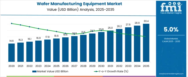
The wafer manufacturing equipment market is projected to grow from USD 18.6 billion in 2025 to USD 30.4 billion in 2035, reflecting a CAGR of 5.0%. During the early adoption phase (2020–2024), the market expanded gradually from USD 14.6 billion to USD 18.6 billion as new equipment and processes were introduced and tested by semiconductor manufacturers. Pilot installations were deployed to evaluate yield improvement, production efficiency, and process reliability. In 2025, the market is expected to reach USD 18.6 billion, with wider integration into fabrication facilities. Initial adoption is being supported by strategic investments and capacity planning by leading chip manufacturers.
From 2025 to 2035, the market is expected to transition through scaling (2025–2030) and consolidation (2030–2035). By 2030, the market is projected to surpass USD 22.7 billion, driven by expanded deployment across semiconductor fabrication plants and enhanced production line utilization. During the consolidation phase, growth is forecast to moderate toward USD 30.4 billion by 2035 as leading equipment suppliers strengthen their market positions and smaller players consolidate or exit. The 5.0% CAGR indicates steady expansion, establishing the market as a standard solution for wafer fabrication, process control, and production efficiency across multiple semiconductor manufacturing facilities.
| Metric | Value |
|---|---|
| Wafer Manufacturing Equipment Market Estimated Value in (2025 E) | USD 18.6 billion |
| Wafer Manufacturing Equipment Market Forecast Value in (2035 F) | USD 30.4 billion |
| Forecast CAGR (2025 to 2035) | 5.0% |
The wafer manufacturing equipment market is influenced by several parent markets, each contributing to overall growth. The semiconductor fabrication sector is estimated to drive approximately 35%, as equipment is deployed to produce wafers for integrated circuits. Semiconductor design and development are considered responsible for 20%, as wafer specifications and process requirements are defined by chip designers. Wafer material and substrate production is assessed to account for 15%, as high-quality silicon and alternative materials are supplied for fabrication. Photolithography and patterning services are estimated to influence 10%, as masks and alignment systems are applied during wafer processing. Inspection and metrology solutions contribute around 7%, as wafers are monitored for defects and process control. Process chemicals and consumables are evaluated at 5%, as etchants, photoresists, and cleaning agents are utilized during fabrication. Equipment maintenance and calibration services account for 5%, as operational efficiency and uptime are maintained. Lastly, research and consulting services are estimated at 3%, as process optimization and technology guidance are provided to wafer manufacturers.
The Wafer Manufacturing Equipment market is witnessing robust growth, driven by the rapid expansion of semiconductor production and increasing demand for advanced electronics. The current market scenario reflects strong adoption of high-precision manufacturing equipment that supports larger wafer sizes and tighter process tolerances. Investments in electronics manufacturing, including memory, logic, and foundry operations, are driving the deployment of advanced wafer cleaning, etching, and deposition systems.
Growth is also being fueled by rising demand for miniaturized devices, high-performance computing, and next-generation consumer electronics. The need for process efficiency, yield improvement, and defect reduction has encouraged manufacturers to upgrade existing lines and integrate automation with real-time process monitoring.
Looking ahead, the market is expected to benefit from continued investment in semiconductor fabrication capacity expansion, coupled with technological innovations such as extreme ultraviolet lithography and advanced process control systems As global demand for semiconductors rises across automotive, industrial, and consumer sectors, wafer manufacturing equipment is positioned to remain a critical enabler of production scalability and operational efficiency.
The wafer manufacturing equipment market is segmented by type, wafer size, end-use industry, and geographic regions. By type, wafer manufacturing equipment market is divided into Wafer cleaning equipment, Wafer slicing equipment, Wafer lapping & polishing equipment, Wafer inspection equipment, Wafer testing equipment, and Wafer dicing equipment. In terms of wafer size, wafer manufacturing equipment market is classified into 200-300mm, 100-200mm, and Above 300mm. Based on end-use industry, wafer manufacturing equipment market is segmented into Electronics manufacturing, Healthcare & life sciences, Automotive industry, Telecommunications, and Others. Regionally, the wafer manufacturing equipment industry is classified into North America, Latin America, Western Europe, Eastern Europe, Balkan & Baltic Countries, Russia & Belarus, Central Asia, East Asia, South Asia & Pacific, and the Middle East & Africa.
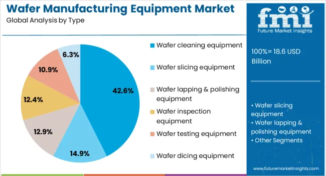
The wafer cleaning equipment type is projected to hold 42.6% of the Wafer Manufacturing Equipment market revenue share in 2025, establishing it as the leading equipment type. This growth has been driven by increasing demand for contamination-free wafers, which is critical for high-performance semiconductor devices. Adoption has been accelerated by the need to reduce defects and improve yield during wafer fabrication, particularly as device geometries shrink and wafer complexity increases.
Wafer cleaning systems are highly valued for their ability to integrate into automated production lines, enabling consistent, high-quality cleaning across diverse wafer sizes. In addition, advances in chemical formulations, megasonic cleaning, and eco-friendly processes have further enhanced the efficiency and sustainability of these systems.
The segment has benefited from the ongoing expansion of semiconductor fabs in Asia and North America, where large-scale production requires reliable, scalable, and low-maintenance cleaning equipment As semiconductor manufacturers continue to prioritize yield optimization and process control, wafer cleaning equipment is expected to sustain its leadership in the market.
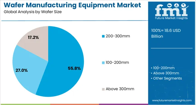
The 200-300mm wafer size segment is expected to capture 55.8% of the overall market revenue in 2025, emerging as the dominant wafer size category. Growth has been driven by widespread adoption in mainstream semiconductor production, including logic, memory, and foundry operations, which favor larger wafers to reduce cost per die and improve manufacturing efficiency.
The shift from smaller wafer diameters to 200-300mm wafers has been motivated by the need to maximize throughput while maintaining high yield rates. Process equipment, including cleaning, deposition, and lithography systems, has increasingly been optimized for these wafer sizes, enabling precise and consistent processing.
Moreover, semiconductor manufacturers have focused on upgrading production lines to accommodate these wafers, driven by global demand for high-performance chips used in data centers, consumer electronics, and automotive applications As the industry continues to pursue scaling, larger wafer sizes remain a key enabler of cost-efficient, high-volume production, reinforcing the segment’s market leadership.
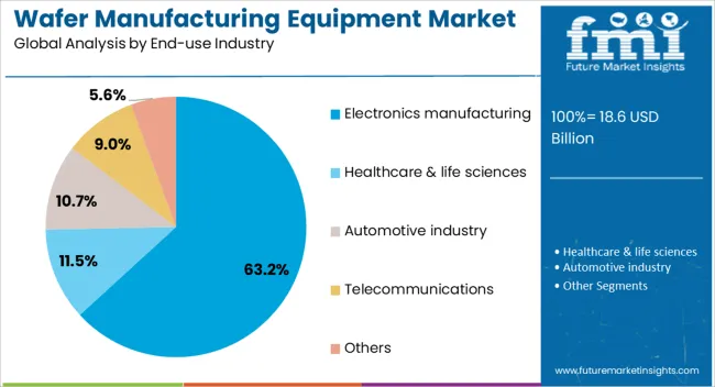
The Electronics Manufacturing end-use industry is anticipated to account for 63.2% of the Wafer Manufacturing Equipment market revenue in 2025, maintaining a leading position among end-use sectors. This dominance is being fueled by the continuous expansion of semiconductor fabrication to meet rising demand for smartphones, computing devices, memory chips, and emerging applications such as artificial intelligence, 5G, and automotive electronics.
Adoption has been accelerated by the need for high-quality, defect-free wafers, which are critical for reliable device performance. Electronics manufacturers are increasingly investing in state-of-the-art wafer fabrication lines, which incorporate automated cleaning, inspection, and process control equipment to enhance yield and throughput.
The integration of software-driven monitoring and real-time analytics has further optimized production efficiency and minimized downtime As consumer demand for high-performance electronic devices grows, coupled with global initiatives to localize semiconductor manufacturing, the electronics manufacturing segment is expected to remain the primary driver of demand for wafer manufacturing equipment, reinforcing its leading market share.
The wafer manufacturing equipment market is expanding due to rising semiconductor demand, miniaturization of chips, and increasing adoption of advanced fabrication technologies. North America and Europe lead with high-precision tools for front-end wafer processing, emphasizing yield improvement and high-volume production. Asia-Pacific is witnessing rapid growth driven by semiconductor foundries, electronics manufacturing, and government incentives. Manufacturers differentiate through process accuracy, automation, throughput, and defect control. Regional variations in technological readiness, R&D investment, and cost sensitivity influence adoption, deployment strategies, and competitive positioning globally.
Adoption of wafer manufacturing equipment is heavily influenced by precision and yield optimization capabilities. North America and Europe prioritize high-end equipment for photolithography, etching, deposition, and inspection, targeting sub-5nm and advanced semiconductor nodes. Asia-Pacific markets increasingly adopt mid-range, high-volume production equipment for consumer electronics and memory chips, balancing cost and precision. Differences in equipment precision affect defect rates, wafer yield, and overall production efficiency. Leading suppliers provide advanced metrology, alignment, and control systems for premium fabs, while regional manufacturers focus on cost-effective, reliable solutions. Precision and yield contrasts shape adoption, productivity, and competitiveness across global wafer manufacturing sectors.
Automation and seamless integration across the wafer fabrication process are critical for operational efficiency. North America and Europe emphasize fully automated process tools and fab-wide integration with manufacturing execution systems (MES) to improve throughput, reduce downtime, and ensure process consistency. Asia-Pacific adoption focuses on semi-automated or modular systems, optimizing cost and flexibility for expanding foundries. Differences in automation levels affect labor dependency, process repeatability, and maintenance requirements. Suppliers providing integrated, intelligent equipment gain higher adoption, while regional players prioritize modular, adaptable systems. Automation and integration contrasts drive operational efficiency, production reliability, and market positioning in wafer manufacturing globally.
High reliability, durability, and low maintenance requirements are essential for wafer manufacturing equipment adoption. North America and Europe demand robust systems with predictive maintenance, remote diagnostics, and long operational lifespans to minimize downtime in advanced semiconductor fabs. Asia-Pacific markets adopt reliable, scalable equipment with moderate maintenance requirements for mass production facilities. Differences in reliability and maintenance affect productivity, total cost of ownership, and process stability. Leading suppliers provide advanced materials, modular designs, and service support for premium applications, while regional manufacturers focus on cost-effective and maintainable solutions. Reliability contrasts shape adoption, operational continuity, and competitive advantage in global wafer manufacturing equipment markets.
Compliance with safety, environmental, and energy efficiency standards significantly influences wafer manufacturing equipment deployment. North America and Europe enforce strict regulations on chemical handling, energy consumption, and cleanroom standards, affecting equipment design, installation, and operating protocols. Asia-Pacific regulations vary; developed regions adhere to international standards, while emerging markets focus on local compliance with practical implementation. Differences in regulatory adherence impact procurement approval, installation timelines, and operational safety. Suppliers offering compliant, energy-efficient equipment gain higher adoption and credibility, while regional producers provide affordable, regulation-aligned solutions. Regulatory contrasts shape adoption, sustainability, and strategic positioning across global wafer manufacturing equipment markets.
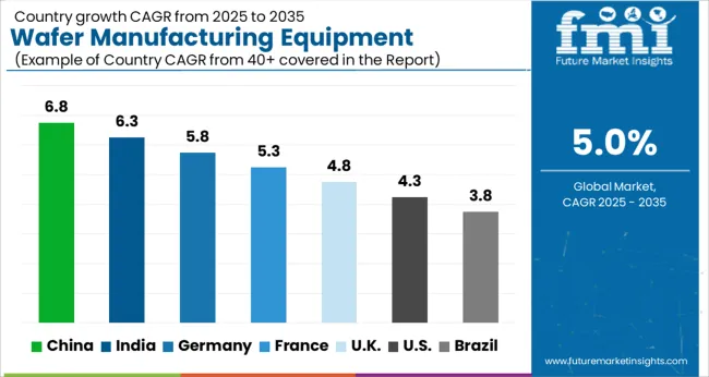
| Country | CAGR |
|---|---|
| China | 6.8% |
| India | 6.3% |
| Germany | 5.8% |
| France | 5.3% |
| UK | 4.8% |
| USA | 4.3% |
| Brazil | 3.8% |
The global wafer manufacturing equipment market was projected to grow at a 5.0% CAGR through 2035, driven by demand in semiconductor fabrication, microelectronics, and precision manufacturing applications. Among BRICS nations, China recorded 6.8% growth as large-scale production and assembly facilities were commissioned and compliance with industrial and safety standards was enforced, while India at 6.3% growth saw expansion of manufacturing units to meet rising regional demand. In the OECD region, Germany at 5.8% maintained substantial output under strict industrial and operational regulations, while the United Kingdom at 4.8% relied on moderate-scale operations for semiconductor and microfabrication applications. The USA, expanding at 4.3%, remained a mature market with steady demand across commercial and industrial microelectronics segments, supported by adherence to federal and state-level quality and safety standards. This report includes insights on 40+ countries; the top five markets are shown here for reference.
The wafer manufacturing equipment market in China is being driven at a CAGR of 6.8% due to the expansion of semiconductor fabrication and electronics production. Advanced deposition, etching, and lithography systems are being adopted to improve wafer quality, yield, and process efficiency. Manufacturers are being encouraged to provide high precision, automated, and energy efficient equipment. Distribution through authorized suppliers, OEMs, and service providers is being maintained. Government initiatives supporting domestic semiconductor production and high tech manufacturing are being followed. Research and development in high resolution, fast processing, and reliable systems is being undertaken to meet industrial demand. China’s large electronics and semiconductor industry is being considered a key factor supporting growth in the wafer manufacturing equipment market.
Wafer manufacturing equipment market in India is being expanded at a CAGR of 6.3% as domestic semiconductor and electronics industries grow. Equipment for deposition, etching, and wafer processing is being adopted to ensure high yield and consistent quality. Manufacturers are being encouraged to supply cost-effective, precise, and energy efficient systems. Distribution through OEMs, authorized suppliers, and service providers is being maintained. Government policies promoting electronics manufacturing and semiconductor self reliance are being followed. Awareness programs and training initiatives are being conducted to ensure proper use and maintenance. Increasing semiconductor fabrication facilities and investments in high tech manufacturing infrastructure are being considered key drivers of market growth in India.
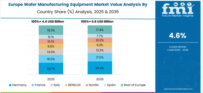
The wafer manufacturing equipment market in Germany is being driven at a CAGR of 5.8% due to high demand from the semiconductor, electronics, and automotive sectors. Deposition, etching, and lithography equipment is being adopted to improve wafer quality, yield, and process efficiency. Manufacturers are being encouraged to provide reliable, automated, and high performance equipment. Distribution through OEMs, industrial suppliers, and service partners is being ensured. Research and development in high precision, energy efficient, and fast processing systems is being conducted. Germany’s strong semiconductor ecosystem, focus on advanced electronics, and strict quality standards are being considered major growth drivers for the wafer manufacturing equipment market.
The United Kingdom wafer manufacturing equipment market is being expanded at a CAGR of 4.8% with adoption of wafer manufacturing equipment in semiconductor, electronics, and R&D applications. Deposition, etching, and lithography systems are being used to ensure high quality, precision, and yield. Manufacturers are being focused on producing durable, automated, and energy efficient equipment. Distribution through authorized suppliers, OEMs, and service providers is being maintained. Awareness campaigns and training programs are being conducted to ensure proper usage and maintenance. Growing demand for microchips, electronics devices, and research applications is being considered a key driver of market growth in the United Kingdom.
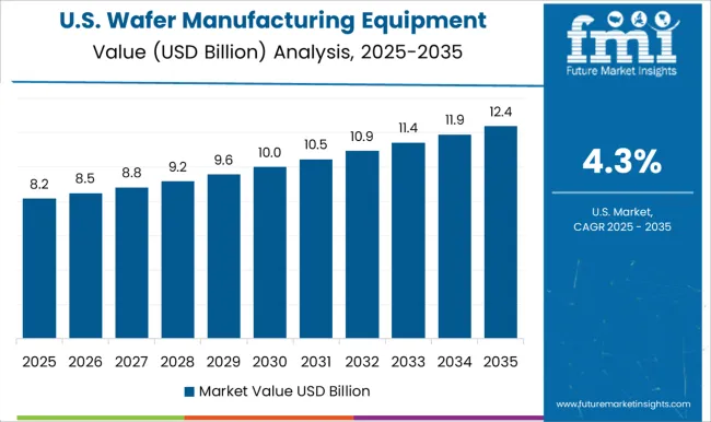
The United States wafer manufacturing equipment market is being driven at a CAGR of 4.3% due to high adoption of wafer manufacturing equipment in semiconductor fabrication, electronics production, and R&D projects. Deposition, etching, and lithography tools are being adopted to improve wafer yield, precision, and processing efficiency. Manufacturers are being encouraged to supply high precision, automated, and energy efficient systems. Distribution through OEMs, authorized suppliers, and service providers is being ensured. Research and development in advanced materials, process automation, and equipment reliability is being conducted. Federal and private investments in semiconductor technology, electronics R&D, and microchip production are being considered key factors supporting market growth in the United States.
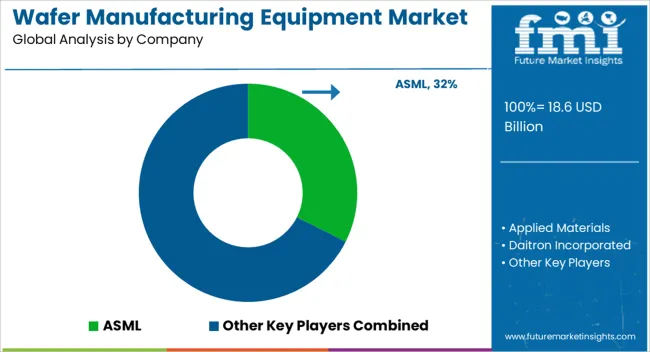
The wafer manufacturing equipment market is heavily influenced by the rapid growth of the semiconductor and electronics industries, where precision and efficiency are critical. Key suppliers in this market include ASML, Applied Materials, Daitron Incorporated, EV Group (EVG), Hitachi High-Tech Corporation, KLA Corporation, and Lam Research Corporation. Advanced wafer fabrication tools are designed, developed, and supplied to support processes such as lithography, etching, deposition, and inspection, enabling high-performance semiconductor devices to be produced at scale. ASML and Applied Materials are recognized for delivering state-of-the-art lithography systems and material processing solutions that enhance wafer throughput and device reliability. Equipment for wafer handling, inspection, and alignment is produced and integrated by Daitron Incorporated and EV Group (EVG), where emphasis is placed on reducing defects and increasing operational efficiency. Continuous innovation is driven to meet the demands of smaller nodes and higher wafer diameters while maintaining precision and minimizing contamination risks. Furthermore, Hitachi High-Tech Corporation, KLA Corporation, and Lam Research Corporation provide critical inspection, metrology, and process control equipment, which are deployed to monitor wafer quality and ensure consistent manufacturing outcomes. Research and development are consistently conducted to introduce automation, AI-assisted process optimization, and energy-efficient systems, helping manufacturers achieve higher yield and lower production costs. Market expansion is supported by increasing demand for semiconductors in consumer electronics, automotive, data centers, and renewable energy applications, with these leading suppliers setting technological standards and driving advancements across the wafer manufacturing ecosystem.
| Item | Value |
|---|---|
| Quantitative Units | USD 18.6 Billion |
| Type | Wafer cleaning equipment, Wafer slicing equipment, Wafer lapping & polishing equipment, Wafer inspection equipment, Wafer testing equipment, and Wafer dicing equipment |
| Wafer Size | 200-300mm, 100-200mm, and Above 300mm |
| End-use Industry | Electronics manufacturing, Healthcare & life sciences, Automotive industry, Telecommunications, and Others |
| Regions Covered | North America, Europe, Asia-Pacific, Latin America, Middle East & Africa |
| Country Covered | United States, Canada, Germany, France, United Kingdom, China, Japan, India, Brazil, South Africa |
| Key Companies Profiled | ASML, Applied Materials, Daitron Incorporated, EV Group (EVG), Hitachi High-Tech Corporation, KLA Corporation, and Lam Research Corporation |
| Additional Attributes | Dollar sales vary by equipment type, including crystal pullers, slicers, polishing machines, and cleaning systems; by technology, such as silicon, gallium arsenide, and silicon carbide wafer manufacturing; by application, spanning semiconductors, MEMS, and photovoltaic cells; by end-use industry, covering semiconductor fabs, electronics manufacturers, and research labs; by region, led by North America, Europe, and Asia-Pacific. Growth is driven by rising semiconductor demand and advanced wafer fabrication requirements. |
The global wafer manufacturing equipment market is estimated to be valued at USD 18.6 billion in 2025.
The market size for the wafer manufacturing equipment market is projected to reach USD 30.4 billion by 2035.
The wafer manufacturing equipment market is expected to grow at a 5.0% CAGR between 2025 and 2035.
The key product types in wafer manufacturing equipment market are wafer cleaning equipment, wafer slicing equipment, wafer lapping & polishing equipment, wafer inspection equipment, wafer testing equipment and wafer dicing equipment.
In terms of wafer size, 200-300mm segment to command 55.8% share in the wafer manufacturing equipment market in 2025.

Our Research Products

The "Full Research Suite" delivers actionable market intel, deep dives on markets or technologies, so clients act faster, cut risk, and unlock growth.

The Leaderboard benchmarks and ranks top vendors, classifying them as Established Leaders, Leading Challengers, or Disruptors & Challengers.

Locates where complements amplify value and substitutes erode it, forecasting net impact by horizon

We deliver granular, decision-grade intel: market sizing, 5-year forecasts, pricing, adoption, usage, revenue, and operational KPIs—plus competitor tracking, regulation, and value chains—across 60 countries broadly.

Spot the shifts before they hit your P&L. We track inflection points, adoption curves, pricing moves, and ecosystem plays to show where demand is heading, why it is changing, and what to do next across high-growth markets and disruptive tech

Real-time reads of user behavior. We track shifting priorities, perceptions of today’s and next-gen services, and provider experience, then pace how fast tech moves from trial to adoption, blending buyer, consumer, and channel inputs with social signals (#WhySwitch, #UX).

Partner with our analyst team to build a custom report designed around your business priorities. From analysing market trends to assessing competitors or crafting bespoke datasets, we tailor insights to your needs.
Supplier Intelligence
Discovery & Profiling
Capacity & Footprint
Performance & Risk
Compliance & Governance
Commercial Readiness
Who Supplies Whom
Scorecards & Shortlists
Playbooks & Docs
Category Intelligence
Definition & Scope
Demand & Use Cases
Cost Drivers
Market Structure
Supply Chain Map
Trade & Policy
Operating Norms
Deliverables
Buyer Intelligence
Account Basics
Spend & Scope
Procurement Model
Vendor Requirements
Terms & Policies
Entry Strategy
Pain Points & Triggers
Outputs
Pricing Analysis
Benchmarks
Trends
Should-Cost
Indexation
Landed Cost
Commercial Terms
Deliverables
Brand Analysis
Positioning & Value Prop
Share & Presence
Customer Evidence
Go-to-Market
Digital & Reputation
Compliance & Trust
KPIs & Gaps
Outputs
Full Research Suite comprises of:
Market outlook & trends analysis
Interviews & case studies
Strategic recommendations
Vendor profiles & capabilities analysis
5-year forecasts
8 regions and 60+ country-level data splits
Market segment data splits
12 months of continuous data updates
DELIVERED AS:
PDF EXCEL ONLINE
Wafer Batch Aligner Market Size and Share Forecast Outlook 2025 to 2035
Wafer Level Packaging Market Size and Share Forecast Outlook 2025 to 2035
Wafer Inspection Market Size and Share Forecast Outlook 2025 to 2035
Wafer Testing Service Market Growth – Trends & Forecast 2024-2034
Wafer Cleaning Equipment Market Growth - Trends & Forecast 2025 to 2035
InP Wafer Market Size and Share Forecast Outlook 2025 to 2035
Thin Wafers Market Analysis - Size, Demand & Growth 2025 to 2035
Thin Wafer Processing and Dicing Equipment Market Size and Share Forecast Outlook 2025 to 2035
Manual Wafer Aligner Market Analysis - Size, Share, and Forecast Outlook 2025 to 2035
Fan-Out Wafer Level Packaging Market Size and Share Forecast Outlook 2025 to 2035
Silicon Epi Wafer Market Size and Share Forecast Outlook 2025 to 2035
Solar Silicon Wafer Market Size and Share Forecast Outlook 2025 to 2035
Semiconductor Wafer Market – Forecast through 2025 to 2035
Solar Photovoltaic Wafer Market
Optical Grade Lithium Tantalate Wafers Market Size and Share Forecast Outlook 2025 to 2035
Manufacturing on Demand for Medical Market Size and Share Forecast Outlook 2025 to 2035
Manufacturing Scale Electrostatic Precipitator Market Size and Share Forecast Outlook 2025 to 2035
Manufacturing Logistics Market Size and Share Forecast Outlook 2025 to 2035
Manufacturing Execution Systems (MES) Market Analysis - Growth, Demand & Forecast 2025 to 2035
Manufacturing Test Systems Market

Thank you!
You will receive an email from our Business Development Manager. Please be sure to check your SPAM/JUNK folder too.
Chat With
MaRIA