The Thin Wafer Processing and Dicing Equipment Market is estimated to be valued at USD 0.8 billion in 2025 and is projected to reach USD 1.6 billion by 2035, registering a compound annual growth rate (CAGR) of 7.0% over the forecast period. A saturation point analysis reveals a steady and gradual increase in growth with signs of stabilization as the market matures. Between 2025 and 2030, the market grows from USD 0.8 billion to USD 1.2 billion, contributing USD 0.4 billion in growth, with a CAGR of 9.2%. This early-phase growth is driven by the increasing demand for advanced semiconductor devices, particularly in the consumer electronics, automotive, and telecommunications sectors. As industries require more precise and smaller components, the need for thin wafer processing and dicing equipment intensifies.
The first inflection point occurs at USD 1.2 billion in 2030, signaling a shift towards more gradual growth. From 2030 to 2035, the market continues to expand from USD 1.2 billion to USD 1.6 billion, contributing USD 0.4 billion in growth, with a slightly lower CAGR of 5.7%. This deceleration reflects the market nearing its saturation point, as the adoption of wafer processing technologies stabilizes and the focus shifts toward replacing older equipment or upgrading existing systems. Despite the slower growth rate, demand remains strong, particularly in regions where the semiconductor industry is rapidly expanding.
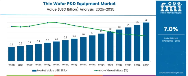
| Metric | Value |
|---|---|
| Thin Wafer Processing and Dicing Equipment Market Estimated Value in (2025 E) | USD 0.8 billion |
| Thin Wafer Processing and Dicing Equipment Market Forecast Value in (2035 F) | USD 1.6 billion |
| Forecast CAGR (2025 to 2035) | 7.0% |
The thin wafer processing and dicing equipment market is experiencing steady growth fueled by the expanding semiconductor industry and the increasing demand for smaller more efficient electronic components. Industry insights highlight the critical role of wafer dicing equipment in achieving precise separation of wafers into individual chips without damaging delicate circuitry.
As semiconductor fabrication advances toward thinner wafers and larger wafer diameters the need for highly accurate and reliable dicing technology becomes more pronounced. The rising production of memory and logic chips especially those using through-silicon via (TSV) technology has further driven demand for specialized equipment capable of handling complex wafer geometries.
Technological improvements in equipment speed precision and automation have enabled manufacturers to boost throughput while maintaining quality. Market expansion is supported by growth in electronics consumption and investments in advanced packaging solutions. Segmental growth is anticipated to be led by dicing equipment within equipment type, 12 inch wafers in wafer size, and memory and logic (TSV) applications.
The thin wafer processing and dicing equipment market is segmented by equipment type, wafer size, application, end-use industry, and geographic regions. By equipment type, the thin wafer processing and dicing equipment market is divided into Dicing equipment and Thinning equipment. In terms of wafer size, the thin wafer processing and dicing equipment market is classified into 12-inch, Less than 4-inch, 5-inch and 6 6-inch, and 8-inch. Based on application, the thin wafer processing and dicing equipment market is segmented into Memory and Logic (TSV), CMOS image sensors, MEMS devices, Power devices, RFID, and Others.
By end-use industry, the thin wafer processing and dicing equipment market is segmented into Consumer electronics, Automotive, Telecommunications, Healthcare, Aerospace & defense, Industrial, and Others. Regionally, the thin wafer processing and dicing equipment industry is classified into North America, Latin America, Western Europe, Eastern Europe, Balkan & Baltic Countries, Russia & Belarus, Central Asia, East Asia, South Asia & Pacific, and the Middle East & Africa.
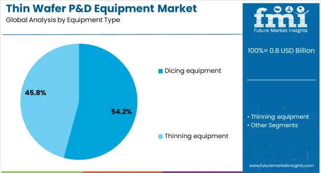
The dicing equipment segment is projected to capture 54.2% of the thin wafer processing and dicing equipment market revenue in 2025, retaining its lead among equipment types. This segment’s growth stems from the essential function dicing equipment performs in precisely cutting wafers into chips without inducing cracks or defects.
As wafer thickness decreases manufacturers require dicing solutions that minimize mechanical stress while maximizing accuracy. The segment has benefited from innovations in laser and blade technologies, enabling cleaner cuts and higher throughput.
The rise in demand for miniaturized devices and advanced semiconductor packaging has reinforced the prominence of dicing equipment in the manufacturing process. With the semiconductor industry’s continuous push for smaller, faster chips, the dicing equipment segment is expected to maintain its dominance.
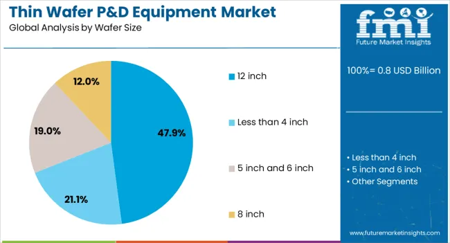
The 12 inch wafer size segment is expected to contribute 47.9% of the market revenue in 2025, establishing it as the largest wafer size category. Larger wafers offer economies of scale enabling more chips to be produced per wafer which reduces manufacturing costs and improves yield.
The transition to 12-inch wafers has been accelerated by semiconductor fabs seeking greater efficiency and capacity. This wafer size is preferred for high-volume production of memory and logic chips as it supports advanced process technologies and tighter geometries.
Equipment compatibility with 12-inch wafers has become a key factor in purchase decisions, driving demand in this segment. As fabs continue upgrading to larger wafer sizes, the 12-inch segment is expected to sustain its market leadership.
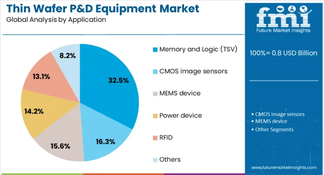
The memory and logic (TSV) application segment is projected to account for 32.5% of the thin wafer processing and dicing equipment market revenue by 2025, positioning it as a significant application area. Growth in this segment is linked to the increasing integration of through-silicon via technology in memory and logic devices, which allows vertical stacking of chips for improved performance and reduced footprint.
The complexity of TSV-enabled devices demands precise dicing and wafer processing equipment to ensure chip integrity. The rising demand for high-speed data processing and memory capacity in consumer electronics and data centers has propelled growth in this application.
As semiconductor manufacturers adopt advanced packaging techniques, the memory and logic (TSV) segment is expected to continue its expansion.
The thin wafer processing and dicing equipment market is experiencing growth due to the increasing demand for semiconductors in various industries such as electronics, automotive, and telecommunications. As technology advances, the need for smaller, thinner, and more efficient wafers is pushing the demand for precision equipment that can process and dice wafers with high accuracy.
This market is being driven by the proliferation of mobile devices, IoT, and emerging technologies like electric vehicles. Despite challenges like high equipment costs and complex manufacturing processes, innovations in wafer processing and dicing techniques continue to fuel market growth.
The primary driver for the growth of the thin wafer processing and dicing equipment market is the increasing demand for smaller and more efficient semiconductor components. As electronic devices continue to shrink in size while requiring higher performance, the need for thinner wafers with precision cuts becomes critical. Wafers that are thinner, lighter, and offer better conductivity are in high demand for applications in mobile devices, consumer electronics, and emerging technologies like electric vehicles and wearable electronics. The automotive industry's shift towards autonomous vehicles, which require advanced semiconductor components, further drives the need for wafer processing and dicing equipment. As the demand for miniaturization continues to rise, the market for thin wafer processing and dicing equipment is expected to grow substantially.
A significant challenge for the thin wafer processing and dicing equipment market is the high cost of equipment. The advanced technology required to process and dice thin wafers with high precision comes at a premium price. This makes it difficult for smaller manufacturers and businesses in emerging markets to adopt this equipment. The technology behind wafer processing and dicing is complex, requiring specialized knowledge and skills to operate and maintain the equipment effectively. The need for constant technological upgrades and innovations further adds to the cost burden. Moreover, the complexity of handling thin wafers, which are fragile and prone to damage during processing, poses another challenge, as manufacturers must ensure high levels of precision and minimize material wastage.
The thin wafer processing and dicing equipment market presents significant opportunities driven by advancements in wafer processing technologies and the expansion of emerging markets. New innovations in wafer processing, such as improved dicing techniques, laser-based cutting technologies, and enhanced material handling systems, offer opportunities for manufacturers to improve efficiency and reduce production costs. The expansion of the semiconductor industry in emerging markets, particularly in Asia-Pacific, is creating new growth avenues for wafer processing and dicing equipment suppliers. As demand for consumer electronics, automotive components, and industrial applications rises, there is significant potential for market growth in these regions. Manufacturers who can offer cost-effective, high-performance solutions to meet the demands of these growing markets will be well-positioned for success.
A key trend in the thin wafer processing and dicing equipment market is the increasing adoption of automation and precision technology. As the demand for higher yields and improved wafer quality grows, manufacturers are focusing on automating the wafer processing and dicing process to increase throughput and reduce human error. Automation not only improves efficiency but also ensures consistency and accuracy, crucial factors when working with thin, fragile wafers. In addition, the integration of real-time monitoring and control systems in wafer processing equipment is gaining popularity, allowing manufacturers to detect issues early in the production process, optimize performance, and minimize material waste. As technology continues to evolve, these trends will shape the future of the thin wafer processing and dicing equipment market, improving the scalability and affordability of semiconductor manufacturing.
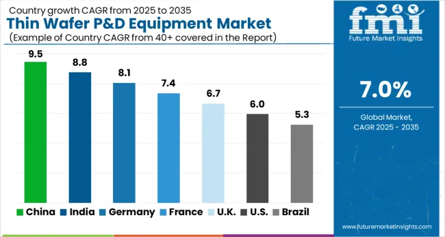
The thin wafer processing and dicing equipment market is projected to grow at a CAGR of 7.0% from 2025 to 2035. China leads the market with a growth rate of 9.5%, followed by India at 8.8%, and France at 7.4%. The United Kingdom is expected to grow at 6.7%, while the United States shows a growth rate of 6.0%. The increasing demand for miniaturized and high-performance electronic devices is driving the need for efficient wafer processing solutions in sectors such as semiconductor manufacturing, telecommunications, and consumer electronics. The market growth is also supported by significant investments in semiconductor production, research and development, and the expansion of the electronics industry in both emerging and developed markets. The analysis covers 40+ countries, with the leading markets shown below.
China is projected to grow at a CAGR of 9.5% through 2035, leading the thin wafer processing and dicing equipment market. The country’s booming electronics and semiconductor sectors are the primary drivers of this growth, as demand for more powerful and miniaturized devices continues to rise. China’s rapidly expanding electronics manufacturing industry, coupled with its focus on becoming a global leader in semiconductor production, is contributing to the growing demand for precision wafer processing technologies. The country’s large consumer electronics market, along with its strong focus on industrial automation and advanced manufacturing technologies, positions China at the forefront of this market.
India is projected to grow at a CAGR of 8.8% through 2035, driven by the rapid expansion of the semiconductor and electronics industries. As India’s industrial sector continues to modernize and grow, the demand for advanced manufacturing technologies, including thin wafer processing and dicing equipment, is on the rise. The growth is further supported by the country's focus on expanding its domestic semiconductor manufacturing capabilities, along with increasing investments in electronics production. The demand for miniaturized and high-performance electronic devices in sectors such as consumer electronics, automotive, and telecommunications is also contributing to the need for efficient and precise wafer processing technologies
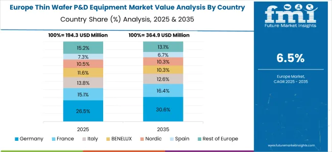
France is projected to grow at a CAGR of 7.4% through 2035, supported by steady demand from the semiconductor and electronics industries. As one of the key markets in Europe, France’s growth is driven by an increasing need for efficient and high-precision wafer processing in advanced electronics, automotive, and telecommunications sectors. The country’s strategic focus on building a robust semiconductor manufacturing infrastructure, combined with its strong research and development activities in electronics and materials science, continues to drive demand for dicing and wafer processing technologies.
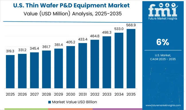
The United States is projected to grow at a CAGR of 6.0% through 2035, with significant demand for thin wafer processing and dicing equipment driven by the growth of the semiconductor and electronics industries. The USA has long been a leader in semiconductor R&D and manufacturing, and the growing demand for miniaturized, high-performance devices is pushing the adoption of more advanced wafer processing technologies. With industries such as automotive, telecommunications, and consumer electronics driving demand for smaller and more efficient chips, the need for high-precision dicing and wafer processing equipment continues to rise.
The United Kingdom is expected to grow at a CAGR of 6.7% through 2035, driven by the expanding demand for high-precision wafer processing and dicing equipment. The UK has a well-established electronics sector, particularly in industries such as telecommunications and consumer electronics, where there is a strong need for miniaturized components. As the demand for advanced, small-form-factor devices rises, so does the need for efficient wafer processing technologies. The UK’s commitment to research and development, particularly in semiconductor and electronics innovation, positions the country as a key player in the growing market for wafer processing and dicing equipment.
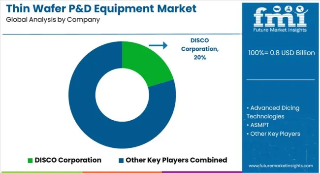
The thin wafer processing and dicing equipment market is driven by leading players that specialize in providing advanced solutions for cutting and processing semiconductor wafers in industries such as electronics, automotive, and telecommunications. DISCO Corporation is a dominant market leader, known for its high-precision wafer dicing equipment and processing tools, which are used extensively in semiconductor manufacturing.
Their innovations in cutting-edge technologies have made them a trusted name in the industry. Advanced Dicing Technologies is another key player, providing advanced equipment for wafer dicing and processing, focusing on high-speed, high-precision solutions tailored to meet the needs of the growing semiconductor sector. ASMPT and AXUS TECHNOLOGY offer highly specialized wafer processing equipment that supports the manufacturing of semiconductors with high efficiency and low cost, focusing on improving throughput and quality control.
Citizen Chiba Precision Co., Ltd. provides innovative, cost-effective wafer dicing solutions, while Dynatex International focuses on precision dicing technologies, offering solutions suitable for a wide range of semiconductor and MEMS applications. EV Group (EVG) and HANMI Semiconductor are recognized for their expertise in advanced wafer processing, providing dicing equipment and solutions for both MEMS and semiconductor device applications.
Han's Laser Technology Co., Ltd. delivers cutting-edge laser dicing systems known for their precision and versatility in thin wafer applications. KLA Corporation and Lam Research Corporation provide advanced wafer inspection and etching equipment, playing a critical role in the overall thin wafer processing and dicing market. Loadpoint Ltd., Modutek Corporation, and NeonTech Co., Ltd. offer cost-effective solutions with a focus on increasing operational efficiency, particularly for high-volume wafer dicing and processing. Panasonic Connect Co., Ltd., Plasma-Therm, and SPTS Technologies Ltd. provide high-quality, reliable wafer processing equipment for semiconductor and microelectronics industries.
Suzhou Delphi Laser Co., Ltd. and Synova SA focus on laser-based dicing solutions, offering high precision for the most delicate wafer processing needs. Tokyo Electron Limited and TOKYO SEIMITSU CO., LTD (Accretech) complete the competitive landscape by providing innovative solutions for wafer thinning, dicing, and precision cutting, catering to a diverse range of industries.
| Item | Value |
|---|---|
| Quantitative Units | USD 0.8 Billion |
| Equipment Type | Dicing equipment and Thinning equipment |
| Wafer Size | 12 inch, Less than 4 inch, 5 inch and 6 inch, and 8 inch |
| Application | Memory and Logic (TSV), CMOS image sensors, MEMS device, Power device, RFID, and Others |
| End-Use Industry | Consumer electronics, Automotive, Telecommunications, Healthcare, Aerospace & defense, Industrial, and Others |
| Regions Covered | North America, Europe, Asia-Pacific, Latin America, Middle East & Africa |
| Country Covered | United States, Canada, Germany, France, United Kingdom, China, Japan, India, Brazil, South Africa |
| Key Companies Profiled | DISCO Corporation, Advanced Dicing Technologies, ASMPT, AXUS TECHNOLOGY, Citizen Chiba Precision Co., Ltd., Dynatex International, EV Group (EVG), HANMI Semiconductor, Han's Laser Technology Co., Ltd., KLA Corporation, Lam Research Corporation, Loadpoint Ltd., Modutek Corporation, NeonTech Co.,Ltd., Panasonic Connect Co., Ltd., Plasma-Therm, SPTS Technologies Ltd., Suzhou Delphi Laser Co., Ltd., Synova SA, Tokyo Electron Limited, and TOKYO SEIMITSU CO., LTD (Accretech) |
| Additional Attributes | Dollar sales by product type (wafer dicing machines, laser dicing equipment, wafer grinders) and end-use segments (semiconductors, MEMS, photonics, optoelectronics, automotive). Demand dynamics are influenced by the increasing complexity of semiconductor devices, the growing need for miniaturized components, and the rising demand for wafer-level packaging in consumer electronics. Regional trends show strong growth in North America and Europe, driven by the presence of key semiconductor manufacturers, while Asia-Pacific is expanding rapidly due to its dominance in semiconductor production and growing demand for wafer processing equipment. |
The global thin wafer processing and dicing equipment market is estimated to be valued at USD 0.8 billion in 2025.
The market size for the thin wafer processing and dicing equipment market is projected to reach USD 1.6 billion by 2035.
The thin wafer processing and dicing equipment market is expected to grow at a 7.0% CAGR between 2025 and 2035.
The key product types in thin wafer processing and dicing equipment market are dicing equipment, thinning equipment, _blade dicing, _laser dicing, _stealth dicing and _plasma dicing.
In terms of wafer size, 12 inch segment to command 47.9% share in the thin wafer processing and dicing equipment market in 2025.
Our Research Products

The "Full Research Suite" delivers actionable market intel, deep dives on markets or technologies, so clients act faster, cut risk, and unlock growth.

The Leaderboard benchmarks and ranks top vendors, classifying them as Established Leaders, Leading Challengers, or Disruptors & Challengers.

Locates where complements amplify value and substitutes erode it, forecasting net impact by horizon

We deliver granular, decision-grade intel: market sizing, 5-year forecasts, pricing, adoption, usage, revenue, and operational KPIs—plus competitor tracking, regulation, and value chains—across 60 countries broadly.

Spot the shifts before they hit your P&L. We track inflection points, adoption curves, pricing moves, and ecosystem plays to show where demand is heading, why it is changing, and what to do next across high-growth markets and disruptive tech

Real-time reads of user behavior. We track shifting priorities, perceptions of today’s and next-gen services, and provider experience, then pace how fast tech moves from trial to adoption, blending buyer, consumer, and channel inputs with social signals (#WhySwitch, #UX).

Partner with our analyst team to build a custom report designed around your business priorities. From analysing market trends to assessing competitors or crafting bespoke datasets, we tailor insights to your needs.
Supplier Intelligence
Discovery & Profiling
Capacity & Footprint
Performance & Risk
Compliance & Governance
Commercial Readiness
Who Supplies Whom
Scorecards & Shortlists
Playbooks & Docs
Category Intelligence
Definition & Scope
Demand & Use Cases
Cost Drivers
Market Structure
Supply Chain Map
Trade & Policy
Operating Norms
Deliverables
Buyer Intelligence
Account Basics
Spend & Scope
Procurement Model
Vendor Requirements
Terms & Policies
Entry Strategy
Pain Points & Triggers
Outputs
Pricing Analysis
Benchmarks
Trends
Should-Cost
Indexation
Landed Cost
Commercial Terms
Deliverables
Brand Analysis
Positioning & Value Prop
Share & Presence
Customer Evidence
Go-to-Market
Digital & Reputation
Compliance & Trust
KPIs & Gaps
Outputs
Full Research Suite comprises of:
Market outlook & trends analysis
Interviews & case studies
Strategic recommendations
Vendor profiles & capabilities analysis
5-year forecasts
8 regions and 60+ country-level data splits
Market segment data splits
12 months of continuous data updates
DELIVERED AS:
PDF EXCEL ONLINE
Wafer Processing Equipment Market Size and Share Forecast Outlook 2025 to 2035
Thin Wafers Market Analysis - Size, Demand & Growth 2025 to 2035
Wafer Cleaning Equipment Market Growth - Trends & Forecast 2025 to 2035
Tea Processing Equipment Market Size and Share Forecast Outlook 2025 to 2035
Wafer Manufacturing Equipment Market Size and Share Forecast Outlook 2025 to 2035
Seed Processing Equipment Market Size and Share Forecast Outlook 2025 to 2035
Meat Processing Equipment Market Size and Share Forecast Outlook 2025 to 2035
Sand Processing Equipment Market Size and Share Forecast Outlook 2025 to 2035
Wine Processing Equipment Market Size and Share Forecast Outlook 2025 to 2035
Fish Processing Equipment Market Size and Share Forecast Outlook 2025 to 2035
Food Processing Equipment Market - Size, Share, and Forecast Outlook 2025 to 2035
Fruit Processing Equipment Market Size and Share Forecast Outlook 2025 to 2035
Dairy Processing Equipment Market Outlook – Growth, Demand & Forecast 2023-2033
Cotton Processing Equipment Market Size and Share Forecast Outlook 2025 to 2035
Bakery Processing Equipment Market Analysis by Product Type, End User, Application & Region: A Forecast for 2025 and 2035
Mineral Processing Equipment Market Size and Share Forecast Outlook 2025 to 2035
Bioprocessing Analytics Equipment Market Size and Share Forecast Outlook 2025 to 2035
Poultry Processing Equipment Market Size and Share Forecast Outlook 2025 to 2035
Beverage Processing Equipment Market Size, Growth, and Forecast 2025 to 2035
Chocolate Processing Equipment Market Size, Growth, and Forecast 2025 to 2035

Thank you!
You will receive an email from our Business Development Manager. Please be sure to check your SPAM/JUNK folder too.
Chat With
MaRIA