Wafer Level Packaging Market
Wafer Level Packaging Market Size and Share Forecast Outlook 2025 to 2035
Wafer Level Packaging Market Size and Share Forecast Outlook 2025 to 2035
The Wafer Level Packaging Market is estimated to be valued at USD 9.5 billion in 2025 and is projected to reach USD 55.6 billion by 2035, registering a compound annual growth rate (CAGR) of 19.3% over the forecast period.
Quick Stats for Wafer Level Packaging Market
- Wafer Level Packaging Market Value (2025): USD 9.5 billion
- Wafer Level Packaging Market Forecast Value (2035): USD 55.6 billion
- Wafer Level Packaging Market Forecast CAGR: 19.3%
- Leading Segment in Wafer Level Packaging Market in 2025: Mobile And Wireless Communications (32.5%)
- Key Growth Regions in Wafer Level Packaging Market: North America, Asia-Pacific, Europe
- Top Key Players in Wafer Level Packaging Market: Fujitsu, Qualcomm Technologies, Inc., Tokyo Electron Ltd., Jiangsu Changjiang Electronics Technology Co. Ltd, Applied Materials, Inc., Amkor Technology, Inc., Lam Research Corporation, ASML Holding N.V, Toshiba Corporation, Deca Technologies
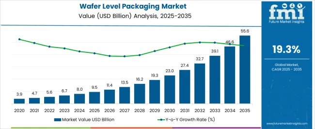
Wafer Level Packaging Market Key Takeaways
| Metric | Value |
|---|---|
| Wafer Level Packaging Market Estimated Value in (2025 E) | USD 9.5 billion |
| Wafer Level Packaging Market Forecast Value in (2035 F) | USD 55.6 billion |
| Forecast CAGR (2025 to 2035) | 19.3% |
Why is the Wafer Level Packaging Market Growing?
The wafer level packaging market is experiencing significant growth driven by the increasing demand for miniaturized, high-performance semiconductor devices across consumer electronics, automotive, and telecommunications industries. Adoption is being fueled by the rapid proliferation of mobile devices, 5G networks, and wearable technology, which require compact, energy-efficient, and high-density packaging solutions. Wafer level packaging is enabling enhanced electrical performance, reduced form factor, and improved thermal management, which are critical for next-generation electronic devices.
Investments in advanced packaging technologies, including fan-out and fan-in solutions, are supporting higher interconnect density and better signal integrity. Growing focus on high-reliability components for mobile, automotive, and industrial applications is accelerating adoption.
The market is further reinforced by increasing research and development activities aimed at improving throughput, reducing production costs, and enhancing yield As electronic systems continue to evolve toward higher performance and smaller sizes, wafer level packaging is expected to remain a key enabler, providing scalable, cost-effective solutions that meet the performance and efficiency demands of modern semiconductor applications.
Segmental Analysis
The wafer level packaging market is segmented by end use, type, and geographic regions. By end use, wafer level packaging market is divided into Mobile And Wireless Communications, Internet Of Things, Automotive, Consumer Electronics, Aerospace, and Healthcare. In terms of type, wafer level packaging market is classified into Fan-Out Wafer Level Package, Fan-In Wafer Level Package, Fan-In Wafer Level Chip Scale Package, Flip Chip, and 3DFOWLP. Regionally, the wafer level packaging industry is classified into North America, Latin America, Western Europe, Eastern Europe, Balkan & Baltic Countries, Russia & Belarus, Central Asia, East Asia, South Asia & Pacific, and the Middle East & Africa.
Insights into the Mobile And Wireless Communications End-Use Segment
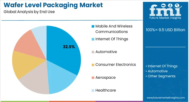
The mobile and wireless communications segment is projected to account for 32.5% of the wafer level packaging market revenue share in 2025, establishing it as the leading end-use category. Its prominence is being driven by the increasing demand for smartphones, tablets, wearable devices, and IoT-enabled gadgets that require high-density, miniaturized packaging solutions.
Wafer level packaging allows for reduced package size, improved electrical performance, and efficient thermal management, making it ideal for mobile and wireless applications. The segment is benefiting from continuous upgrades in mobile technology, such as 5G and high-speed data communication, which require advanced packaging to support higher signal integrity and lower power consumption.
Manufacturers are increasingly adopting wafer level packages to meet stringent performance standards and enhance device reliability in compact form factors Rising demand for multi-functional mobile devices, coupled with the need for high-performance computing and connectivity in wireless applications, is reinforcing this segment’s leadership position in the global wafer level packaging market.
Insights into the Fan-Out Wafer Level Package Type Segment
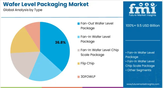
The fan-out wafer level package type is expected to hold 36.8% of the wafer level packaging market revenue share in 2025, making it the dominant package type. Its growth is being driven by the ability to provide higher input-output density, improved thermal performance, and enhanced electrical reliability compared to traditional fan-in packages. Fan-out wafer level packages enable integration of heterogeneous components, allowing complex system-on-chip designs in compact form factors without compromising performance.
The segment benefits from the increasing demand for high-performance computing, mobile, and wireless applications that require reduced package size and superior signal integrity. Continuous advancements in fan-out process technology, including redistribution layers and molding techniques, are improving production yield and enabling cost-effective large-scale adoption.
The flexibility to accommodate diverse device requirements, combined with its superior electrical and thermal characteristics, is reinforcing the segment’s market leadership As demand for next-generation semiconductor devices rises, fan-out wafer level packages are expected to remain the preferred solution for high-density, high-performance applications globally.
Market Overview
Wafer Level Packaging Market Outlook
The wafer-level packaging technology is revolutionizing packaging with innovative thin wafer handling (TWH) technologies. The diverse set of performance materials involved in the wafer-level packaging has made smooth allowances for higher throughput, lower cost, and reduction in form factor for manufacturers. Fully automated solutions are being deployed for high-volume needs of wafer-level packaging.
The utilization of wafer-level packaging allows the chips to continue to reduce in size, provides easier ways to test the functionality of the chips, and streamlines the manufacturing procedures. To reach the utmost goal, the organizations are focusing on finding ways to thin their device wafers before performing complex back-end processes.
To add some edge and innovate the realm of wafer-level packaging, the enterprises are looking to connect with some temporary bonding techniques, in which the wafer is attached to a stable carrier without disrupting the back-end processes. By thinning the wafers, the key players can enable expertise over form factor reduction, increased performance, better heat dissipation, and decreased power consumption.
The technological superiority of wafer-level packaging over traditional packaging approaches is likely to give an upper hand to the manufacturers. Whilst there is no industry standard approach to wafer-level packaging, with rapid advancement in integrated circuit manufacturing processes, fans in wafer-level packaging solutions are likely to gain significant traction in the packaging area.
The prominent players in the wafer-level packaging market are very much focused on their investments in cost-effective, technologically advanced, and more secure products and solutions for various applications, coupled with the silent trends of advanced packaging like wlcsp package, wlcsp process flow, and wafer chip scale package.
The manufacturers can indulge in a broad array of wafer-level packaging capabilities and processes for packaging schemes from fan-out to chip scale to 3D to System-in-Package (SiP). Some of the top players are advancing their manufacturing operations in emerging economies like China, Korea, Taiwan, and Portugal, adjacent to major foundries, enabling the integration of factory logistics and reducing time to market.
It is also observed that for gaining rapid traction in the market, device encapsulation technologies are also being adopted by some of the eminent players, and with the diverse set of technical advances incorporated, along with collaborations made with leading equipment vendors, the biggies are making frequent innovations to provide wafer fabrication equipment for high volume needs in the end-use industries.
Therefore, it can be anticipated that the competitive landscape has lucrative growth prospects, and the wafer-level packaging market is likely to have significant expansion during the forecast period.
Analysis of Wafer Level Packaging Market By Key Countries
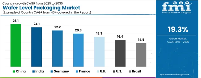
| Country | CAGR |
|---|---|
| China | 26.1% |
| India | 24.1% |
| Germany | 22.2% |
| France | 20.3% |
| UK | 18.3% |
| USA | 16.4% |
| Brazil | 14.5% |
Country-wise Analysis
The Wafer Level Packaging Market is expected to register a CAGR of 19.3% during the forecast period, exhibiting varied country level momentum. China leads with the highest CAGR of 26.1%, followed by India at 24.1%. Developed markets such as Germany, France, and the UK continue to expand steadily, while the USA is likely to grow at consistent rates. Brazil posts the lowest CAGR at 14.5%, yet still underscores a broadly positive trajectory for the global Wafer Level Packaging Market. In 2024, Germany held a dominant revenue in the Western Europe market and is expected to grow with a CAGR of 22.2%. The USA Wafer Level Packaging Market is estimated to be valued at USD 3.5 billion in 2025 and is anticipated to reach a valuation of USD 16.1 billion by 2035. Sales are projected to rise at a CAGR of 16.4% over the forecast period between 2025 and 2035. While Japan and South Korea markets are estimated to be valued at USD 502.5 million and USD 252.5 million respectively in 2025.
Key Players in the Wafer Level Packaging Market
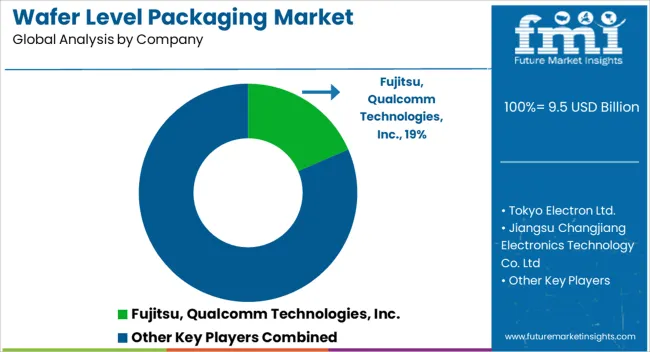
- Fujitsu, Qualcomm Technologies, Inc.
- Tokyo Electron Ltd.
- Jiangsu Changjiang Electronics Technology Co. Ltd
- Applied Materials, Inc.
- Amkor Technology, Inc.
- Lam Research Corporation
- ASML Holding N.V
- Toshiba Corporation
- Deca Technologies
Scope of the Report
| Item | Value |
|---|---|
| Quantitative Units | USD 9.5 Billion |
| End Use | Mobile And Wireless Communications, Internet Of Things, Automotive, Consumer Electronics, Aerospace, and Healthcare |
| Type | Fan-Out Wafer Level Package, Fan-In Wafer Level Package, Fan-In Wafer Level Chip Scale Package, Flip Chip, and 3DFOWLP |
| Regions Covered | North America, Europe, Asia-Pacific, Latin America, Middle East & Africa |
| Country Covered | United States, Canada, Germany, France, United Kingdom, China, Japan, India, Brazil, South Africa |
| Key Companies Profiled | Fujitsu, Qualcomm Technologies, Inc., Tokyo Electron Ltd., Jiangsu Changjiang Electronics Technology Co. Ltd, Applied Materials, Inc., Amkor Technology, Inc., Lam Research Corporation, ASML Holding N.V, Toshiba Corporation, and Deca Technologies |
Wafer Level Packaging Market by Segments
End Use:
- Mobile And Wireless Communications
- Internet Of Things
- Automotive
- Consumer Electronics
- Aerospace
- Healthcare
Type:
- Fan-Out Wafer Level Package
- Fan-In Wafer Level Package
- Fan-In Wafer Level Chip Scale Package
- Flip Chip
- 3DFOWLP
Region:
- North America
- USA
- Canada
- Mexico
- Latin America
- Brazil
- Chile
- Rest of Latin America
- Western Europe
- Germany
- UK
- Italy
- Spain
- France
- Nordic
- BENELUX
- Rest of Western Europe
- Eastern Europe
- Russia
- Poland
- Hungary
- Balkan & Baltic
- Rest of Eastern Europe
- East Asia
- China
- Japan
- South Korea
- South Asia and Pacific
- India
- ASEAN
- Australia & New Zealand
- Rest of South Asia and Pacific
- Middle East & Africa
- Kingdom of Saudi Arabia
- Other GCC Countries
- Turkiye
- South Africa
- Other African Union
- Rest of Middle East & Africa
Frequently Asked Questions
How big is the wafer level packaging market in 2025?
The global wafer level packaging market is estimated to be valued at USD 9.5 billion in 2025.
What will be the size of wafer level packaging market in 2035?
The market size for the wafer level packaging market is projected to reach USD 55.6 billion by 2035.
How much will be the wafer level packaging market growth between 2025 and 2035?
The wafer level packaging market is expected to grow at a 19.3% CAGR between 2025 and 2035.
What are the key product types in the wafer level packaging market?
The key product types in wafer level packaging market are mobile and wireless communications, internet of things, automotive, consumer electronics, aerospace and healthcare.
Which type segment to contribute significant share in the wafer level packaging market in 2025?
In terms of type, fan-out wafer level package segment to command 36.8% share in the wafer level packaging market in 2025.
Table of Content
- Executive Summary
- Global Market Outlook
- Demand-side Trends
- Supply-side Trends
- Technology Roadmap Analysis
- Analysis and Recommendations
- Market Overview
- Market Coverage / Taxonomy
- Market Definition / Scope / Limitations
- Market Background
- Market Dynamics
- Drivers
- Restraints
- Opportunity
- Trends
- Scenario Forecast
- Demand in Optimistic Scenario
- Demand in Likely Scenario
- Demand in Conservative Scenario
- Opportunity Map Analysis
- Product Life Cycle Analysis
- Supply Chain Analysis
- Investment Feasibility Matrix
- Value Chain Analysis
- PESTLE and Porter’s Analysis
- Regulatory Landscape
- Regional Parent Market Outlook
- Production and Consumption Statistics
- Import and Export Statistics
- Market Dynamics
- Global Market Analysis 2020 to 2024 and Forecast, 2025 to 2035
- Historical Market Size Value (USD Million) Analysis, 2020 to 2024
- Current and Future Market Size Value (USD Million) Projections, 2025 to 2035
- Y-o-Y Growth Trend Analysis
- Absolute $ Opportunity Analysis
- Global Market Pricing Analysis 2020 to 2024 and Forecast 2025 to 2035
- Global Market Analysis 2020 to 2024 and Forecast 2025 to 2035, By End Use
- Introduction / Key Findings
- Historical Market Size Value (USD Million) Analysis By End Use , 2020 to 2024
- Current and Future Market Size Value (USD Million) Analysis and Forecast By End Use , 2025 to 2035
- Mobile And Wireless Communications
- Internet Of Things
- Automotive
- Consumer Electronics
- Aerospace
- Healthcare
- Y-o-Y Growth Trend Analysis By End Use , 2020 to 2024
- Absolute $ Opportunity Analysis By End Use , 2025 to 2035
- Global Market Analysis 2020 to 2024 and Forecast 2025 to 2035, By Type
- Introduction / Key Findings
- Historical Market Size Value (USD Million) Analysis By Type, 2020 to 2024
- Current and Future Market Size Value (USD Million) Analysis and Forecast By Type, 2025 to 2035
- Fan-Out Wafer Level Package
- Fan-In Wafer Level Package
- Fan-In Wafer Level Chip Scale Package
- Flip Chip
- 3DFOWLP
- Y-o-Y Growth Trend Analysis By Type, 2020 to 2024
- Absolute $ Opportunity Analysis By Type, 2025 to 2035
- Global Market Analysis 2020 to 2024 and Forecast 2025 to 2035, By Region
- Introduction
- Historical Market Size Value (USD Million) Analysis By Region, 2020 to 2024
- Current Market Size Value (USD Million) Analysis and Forecast By Region, 2025 to 2035
- North America
- Latin America
- Western Europe
- Eastern Europe
- East Asia
- South Asia and Pacific
- Middle East & Africa
- Market Attractiveness Analysis By Region
- North America Market Analysis 2020 to 2024 and Forecast 2025 to 2035, By Country
- Historical Market Size Value (USD Million) Trend Analysis By Market Taxonomy, 2020 to 2024
- Market Size Value (USD Million) Forecast By Market Taxonomy, 2025 to 2035
- By Country
- USA
- Canada
- Mexico
- By End Use
- By Type
- By Country
- Market Attractiveness Analysis
- By Country
- By End Use
- By Type
- Key Takeaways
- Latin America Market Analysis 2020 to 2024 and Forecast 2025 to 2035, By Country
- Historical Market Size Value (USD Million) Trend Analysis By Market Taxonomy, 2020 to 2024
- Market Size Value (USD Million) Forecast By Market Taxonomy, 2025 to 2035
- By Country
- Brazil
- Chile
- Rest of Latin America
- By End Use
- By Type
- By Country
- Market Attractiveness Analysis
- By Country
- By End Use
- By Type
- Key Takeaways
- Western Europe Market Analysis 2020 to 2024 and Forecast 2025 to 2035, By Country
- Historical Market Size Value (USD Million) Trend Analysis By Market Taxonomy, 2020 to 2024
- Market Size Value (USD Million) Forecast By Market Taxonomy, 2025 to 2035
- By Country
- Germany
- UK
- Italy
- Spain
- France
- Nordic
- BENELUX
- Rest of Western Europe
- By End Use
- By Type
- By Country
- Market Attractiveness Analysis
- By Country
- By End Use
- By Type
- Key Takeaways
- Eastern Europe Market Analysis 2020 to 2024 and Forecast 2025 to 2035, By Country
- Historical Market Size Value (USD Million) Trend Analysis By Market Taxonomy, 2020 to 2024
- Market Size Value (USD Million) Forecast By Market Taxonomy, 2025 to 2035
- By Country
- Russia
- Poland
- Hungary
- Balkan & Baltic
- Rest of Eastern Europe
- By End Use
- By Type
- By Country
- Market Attractiveness Analysis
- By Country
- By End Use
- By Type
- Key Takeaways
- East Asia Market Analysis 2020 to 2024 and Forecast 2025 to 2035, By Country
- Historical Market Size Value (USD Million) Trend Analysis By Market Taxonomy, 2020 to 2024
- Market Size Value (USD Million) Forecast By Market Taxonomy, 2025 to 2035
- By Country
- China
- Japan
- South Korea
- By End Use
- By Type
- By Country
- Market Attractiveness Analysis
- By Country
- By End Use
- By Type
- Key Takeaways
- South Asia and Pacific Market Analysis 2020 to 2024 and Forecast 2025 to 2035, By Country
- Historical Market Size Value (USD Million) Trend Analysis By Market Taxonomy, 2020 to 2024
- Market Size Value (USD Million) Forecast By Market Taxonomy, 2025 to 2035
- By Country
- India
- ASEAN
- Australia & New Zealand
- Rest of South Asia and Pacific
- By End Use
- By Type
- By Country
- Market Attractiveness Analysis
- By Country
- By End Use
- By Type
- Key Takeaways
- Middle East & Africa Market Analysis 2020 to 2024 and Forecast 2025 to 2035, By Country
- Historical Market Size Value (USD Million) Trend Analysis By Market Taxonomy, 2020 to 2024
- Market Size Value (USD Million) Forecast By Market Taxonomy, 2025 to 2035
- By Country
- Kingdom of Saudi Arabia
- Other GCC Countries
- Turkiye
- South Africa
- Other African Union
- Rest of Middle East & Africa
- By End Use
- By Type
- By Country
- Market Attractiveness Analysis
- By Country
- By End Use
- By Type
- Key Takeaways
- Key Countries Market Analysis
- USA
- Pricing Analysis
- Market Share Analysis, 2024
- By End Use
- By Type
- Canada
- Pricing Analysis
- Market Share Analysis, 2024
- By End Use
- By Type
- Mexico
- Pricing Analysis
- Market Share Analysis, 2024
- By End Use
- By Type
- Brazil
- Pricing Analysis
- Market Share Analysis, 2024
- By End Use
- By Type
- Chile
- Pricing Analysis
- Market Share Analysis, 2024
- By End Use
- By Type
- Germany
- Pricing Analysis
- Market Share Analysis, 2024
- By End Use
- By Type
- UK
- Pricing Analysis
- Market Share Analysis, 2024
- By End Use
- By Type
- Italy
- Pricing Analysis
- Market Share Analysis, 2024
- By End Use
- By Type
- Spain
- Pricing Analysis
- Market Share Analysis, 2024
- By End Use
- By Type
- France
- Pricing Analysis
- Market Share Analysis, 2024
- By End Use
- By Type
- India
- Pricing Analysis
- Market Share Analysis, 2024
- By End Use
- By Type
- ASEAN
- Pricing Analysis
- Market Share Analysis, 2024
- By End Use
- By Type
- Australia & New Zealand
- Pricing Analysis
- Market Share Analysis, 2024
- By End Use
- By Type
- China
- Pricing Analysis
- Market Share Analysis, 2024
- By End Use
- By Type
- Japan
- Pricing Analysis
- Market Share Analysis, 2024
- By End Use
- By Type
- South Korea
- Pricing Analysis
- Market Share Analysis, 2024
- By End Use
- By Type
- Russia
- Pricing Analysis
- Market Share Analysis, 2024
- By End Use
- By Type
- Poland
- Pricing Analysis
- Market Share Analysis, 2024
- By End Use
- By Type
- Hungary
- Pricing Analysis
- Market Share Analysis, 2024
- By End Use
- By Type
- Kingdom of Saudi Arabia
- Pricing Analysis
- Market Share Analysis, 2024
- By End Use
- By Type
- Turkiye
- Pricing Analysis
- Market Share Analysis, 2024
- By End Use
- By Type
- South Africa
- Pricing Analysis
- Market Share Analysis, 2024
- By End Use
- By Type
- USA
- Market Structure Analysis
- Competition Dashboard
- Competition Benchmarking
- Market Share Analysis of Top Players
- By Regional
- By End Use
- By Type
- Competition Analysis
- Competition Deep Dive
- Fujitsu, Qualcomm Technologies, Inc.
- Overview
- Product Portfolio
- Profitability by Market Segments (Product/Age /Sales Channel/Region)
- Sales Footprint
- Strategy Overview
- Marketing Strategy
- Product Strategy
- Channel Strategy
- Tokyo Electron Ltd.
- Jiangsu Changjiang Electronics Technology Co. Ltd
- Applied Materials, Inc.
- Amkor Technology, Inc.
- Lam Research Corporation
- ASML Holding N.V
- Toshiba Corporation
- Deca Technologies
- Fujitsu, Qualcomm Technologies, Inc.
- Competition Deep Dive
- Assumptions & Acronyms Used
- Research Methodology
List of Tables
- Table 1: Global Market Value (USD Million) Forecast by Region, 2020-2035
- Table 2: Global Market Value (USD Million) Forecast by End Use , 2020-2035
- Table 3: Global Market Value (USD Million) Forecast by Type, 2020-2035
- Table 4: North America Market Value (USD Million) Forecast by Country, 2020-2035
- Table 5: North America Market Value (USD Million) Forecast by End Use , 2020-2035
- Table 6: North America Market Value (USD Million) Forecast by Type, 2020-2035
- Table 7: Latin America Market Value (USD Million) Forecast by Country, 2020-2035
- Table 8: Latin America Market Value (USD Million) Forecast by End Use , 2020-2035
- Table 9: Latin America Market Value (USD Million) Forecast by Type, 2020-2035
- Table 10: Western Europe Market Value (USD Million) Forecast by Country, 2020-2035
- Table 11: Western Europe Market Value (USD Million) Forecast by End Use , 2020-2035
- Table 12: Western Europe Market Value (USD Million) Forecast by Type, 2020-2035
- Table 13: Eastern Europe Market Value (USD Million) Forecast by Country, 2020-2035
- Table 14: Eastern Europe Market Value (USD Million) Forecast by End Use , 2020-2035
- Table 15: Eastern Europe Market Value (USD Million) Forecast by Type, 2020-2035
- Table 16: East Asia Market Value (USD Million) Forecast by Country, 2020-2035
- Table 17: East Asia Market Value (USD Million) Forecast by End Use , 2020-2035
- Table 18: East Asia Market Value (USD Million) Forecast by Type, 2020-2035
- Table 19: South Asia and Pacific Market Value (USD Million) Forecast by Country, 2020-2035
- Table 20: South Asia and Pacific Market Value (USD Million) Forecast by End Use , 2020-2035
- Table 21: South Asia and Pacific Market Value (USD Million) Forecast by Type, 2020-2035
- Table 22: Middle East & Africa Market Value (USD Million) Forecast by Country, 2020-2035
- Table 23: Middle East & Africa Market Value (USD Million) Forecast by End Use , 2020-2035
- Table 24: Middle East & Africa Market Value (USD Million) Forecast by Type, 2020-2035
List of Figures
- Figure 1: Global Market Pricing Analysis
- Figure 2: Global Market Value (USD Million) Forecast 2020-2035
- Figure 3: Global Market Value Share and BPS Analysis by End Use , 2025 and 2035
- Figure 4: Global Market Y-o-Y Growth Comparison by End Use , 2025-2035
- Figure 5: Global Market Attractiveness Analysis by End Use
- Figure 6: Global Market Value Share and BPS Analysis by Type, 2025 and 2035
- Figure 7: Global Market Y-o-Y Growth Comparison by Type, 2025-2035
- Figure 8: Global Market Attractiveness Analysis by Type
- Figure 9: Global Market Value (USD Million) Share and BPS Analysis by Region, 2025 and 2035
- Figure 10: Global Market Y-o-Y Growth Comparison by Region, 2025-2035
- Figure 11: Global Market Attractiveness Analysis by Region
- Figure 12: North America Market Incremental Dollar Opportunity, 2025-2035
- Figure 13: Latin America Market Incremental Dollar Opportunity, 2025-2035
- Figure 14: Western Europe Market Incremental Dollar Opportunity, 2025-2035
- Figure 15: Eastern Europe Market Incremental Dollar Opportunity, 2025-2035
- Figure 16: East Asia Market Incremental Dollar Opportunity, 2025-2035
- Figure 17: South Asia and Pacific Market Incremental Dollar Opportunity, 2025-2035
- Figure 18: Middle East & Africa Market Incremental Dollar Opportunity, 2025-2035
- Figure 19: North America Market Value Share and BPS Analysis by Country, 2025 and 2035
- Figure 20: North America Market Value Share and BPS Analysis by End Use , 2025 and 2035
- Figure 21: North America Market Y-o-Y Growth Comparison by End Use , 2025-2035
- Figure 22: North America Market Attractiveness Analysis by End Use
- Figure 23: North America Market Value Share and BPS Analysis by Type, 2025 and 2035
- Figure 24: North America Market Y-o-Y Growth Comparison by Type, 2025-2035
- Figure 25: North America Market Attractiveness Analysis by Type
- Figure 26: Latin America Market Value Share and BPS Analysis by Country, 2025 and 2035
- Figure 27: Latin America Market Value Share and BPS Analysis by End Use , 2025 and 2035
- Figure 28: Latin America Market Y-o-Y Growth Comparison by End Use , 2025-2035
- Figure 29: Latin America Market Attractiveness Analysis by End Use
- Figure 30: Latin America Market Value Share and BPS Analysis by Type, 2025 and 2035
- Figure 31: Latin America Market Y-o-Y Growth Comparison by Type, 2025-2035
- Figure 32: Latin America Market Attractiveness Analysis by Type
- Figure 33: Western Europe Market Value Share and BPS Analysis by Country, 2025 and 2035
- Figure 34: Western Europe Market Value Share and BPS Analysis by End Use , 2025 and 2035
- Figure 35: Western Europe Market Y-o-Y Growth Comparison by End Use , 2025-2035
- Figure 36: Western Europe Market Attractiveness Analysis by End Use
- Figure 37: Western Europe Market Value Share and BPS Analysis by Type, 2025 and 2035
- Figure 38: Western Europe Market Y-o-Y Growth Comparison by Type, 2025-2035
- Figure 39: Western Europe Market Attractiveness Analysis by Type
- Figure 40: Eastern Europe Market Value Share and BPS Analysis by Country, 2025 and 2035
- Figure 41: Eastern Europe Market Value Share and BPS Analysis by End Use , 2025 and 2035
- Figure 42: Eastern Europe Market Y-o-Y Growth Comparison by End Use , 2025-2035
- Figure 43: Eastern Europe Market Attractiveness Analysis by End Use
- Figure 44: Eastern Europe Market Value Share and BPS Analysis by Type, 2025 and 2035
- Figure 45: Eastern Europe Market Y-o-Y Growth Comparison by Type, 2025-2035
- Figure 46: Eastern Europe Market Attractiveness Analysis by Type
- Figure 47: East Asia Market Value Share and BPS Analysis by Country, 2025 and 2035
- Figure 48: East Asia Market Value Share and BPS Analysis by End Use , 2025 and 2035
- Figure 49: East Asia Market Y-o-Y Growth Comparison by End Use , 2025-2035
- Figure 50: East Asia Market Attractiveness Analysis by End Use
- Figure 51: East Asia Market Value Share and BPS Analysis by Type, 2025 and 2035
- Figure 52: East Asia Market Y-o-Y Growth Comparison by Type, 2025-2035
- Figure 53: East Asia Market Attractiveness Analysis by Type
- Figure 54: South Asia and Pacific Market Value Share and BPS Analysis by Country, 2025 and 2035
- Figure 55: South Asia and Pacific Market Value Share and BPS Analysis by End Use , 2025 and 2035
- Figure 56: South Asia and Pacific Market Y-o-Y Growth Comparison by End Use , 2025-2035
- Figure 57: South Asia and Pacific Market Attractiveness Analysis by End Use
- Figure 58: South Asia and Pacific Market Value Share and BPS Analysis by Type, 2025 and 2035
- Figure 59: South Asia and Pacific Market Y-o-Y Growth Comparison by Type, 2025-2035
- Figure 60: South Asia and Pacific Market Attractiveness Analysis by Type
- Figure 61: Middle East & Africa Market Value Share and BPS Analysis by Country, 2025 and 2035
- Figure 62: Middle East & Africa Market Value Share and BPS Analysis by End Use , 2025 and 2035
- Figure 63: Middle East & Africa Market Y-o-Y Growth Comparison by End Use , 2025-2035
- Figure 64: Middle East & Africa Market Attractiveness Analysis by End Use
- Figure 65: Middle East & Africa Market Value Share and BPS Analysis by Type, 2025 and 2035
- Figure 66: Middle East & Africa Market Y-o-Y Growth Comparison by Type, 2025-2035
- Figure 67: Middle East & Africa Market Attractiveness Analysis by Type
- Figure 68: Global Market - Tier Structure Analysis
- Figure 69: Global Market - Company Share Analysis
Full Research Suite comprises of:
Market outlook & trends analysis
Interviews & case studies
Strategic recommendations
Vendor profiles & capabilities analysis
5-year forecasts
8 regions and 60+ country-level data splits
Market segment data splits
12 months of continuous data updates
DELIVERED AS:
PDF EXCEL ONLINE

