The fan-out wafer level packaging market is estimated to be valued at USD 3.3 billion in 2025 and is projected to reach USD 8.6 billion by 2035, registering a compound annual growth rate (CAGR) of 10.0% over the forecast period. The first five-year growth block for fan-out wafer-level packaging is projected from USD 3.3 billion in 2025 to USD 5.4 billion in 2030. Values are expected to move to 3.7 billion in 2026, 4.0 billion in 2027, 4.4 billion in 2028, and 4.9 billion in 2029 before reaching 5.4 billion. Momentum is being shaped by advanced packaging needs in mobile application processors, RF front ends, power management ICs, and automotive electronics.
Redistribution layer density, warpage control, molded underfill quality, and known good die supply are being prioritized. This growth block establishes a firm base for wider heterogeneous integration and chiplet-based system in package designs. The broader trajectory toward USD 8.6 billion by 2035 at a 10% CAGR is being underwritten by capacity adds at OSATs and foundries, tighter design rules in RDL, and improved thermo-mechanical reliability of large body packages. Differentiation is likely to be earned through yield management, copper RDL lifetime, fan out on substrate variants, and seamless chip to package co-design with EDA partners. Procurement choices are influenced by total cost per input-output, cycle time, and test coverage. Suppliers with material depth and ecosystem partnerships will capture a superior share of the absolute dollar opportunity.
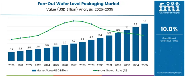
| Metric | Value |
|---|---|
| Fan-Out Wafer Level Packaging Market Estimated Value in (2025 E) | USD 3.3 billion |
| Fan-Out Wafer Level Packaging Market Forecast Value in (2035 F) | USD 8.6 billion |
| Forecast CAGR (2025 to 2035) | 10.0% |
The fan out wafer level packaging segment is estimated to account for about 15% of the advanced packaging market, around 8% of the semiconductor packaging market, close to 32% of the wafer level packaging market, nearly 12% of the system in package market, and roughly 14% of the heterogeneous integration market. These proportions aggregate to approximately 81% across the listed parent categories.
Value has been recognized in substrate elimination and redistribution layer freedom that enable compact footprints with strong electrical performance. FO WLP functions as a practical bridge between flip chip packaging and 2.5D pathways, where bill of materials, yield learning, and volume scaling are decisive. Buyer preferences are often shaped by line width and space capability, mold compound stability, warpage control, underfill-free reliability, and panel-level process maturity at OSAT and foundry partners. Demand has been reinforced by handset and edge compute programs that require thin profiles without sacrificing electromigration margins or signal integrity.
As process design kits, material stacks, and simulation models mature, FO WLP is expected to secure deeper specification in advanced packaging roadmaps, guiding capital toward RDL tooling, panel lines, plasma dicing, and known good die strategies that support predictable ramps and competitive total cost.
The fan-out wafer level packaging market is experiencing significant growth due to its ability to deliver higher performance, miniaturization, and improved thermal management in semiconductor devices. Increasing demand from sectors such as consumer electronics, automotive, and telecommunications is accelerating market expansion. The market is driven by trends emphasizing smaller form factors, enhanced electrical performance, and cost-effectiveness compared to traditional packaging techniques.
The rise in complex integrated circuits with increased input/output counts necessitates advanced packaging solutions like fan-out wafer level packaging, which supports better signal integrity and power efficiency. Strategic partnerships and investments by OSAT providers to expand capabilities and geographic reach are further boosting market dynamics.
Additionally, growing adoption in consumer electronics is propelled by the proliferation of smartphones, wearable devices, and IoT applications that require compact and high-performance packages. As semiconductor manufacturers continue to push technological boundaries, fan-out wafer level packaging is positioned for sustained growth fueled by innovation and rising end-use demand.
The fan-out wafer level packaging market is segmented by process type, business model, application, and geographic regions. By process type, fan-out wafer level packaging market is divided into standard-density packaging, high-density packaging, and bumping. In terms of business model, fan-out wafer level packaging market is classified into OSAT, Foundry, and IDM.
Based on application, fan-out wafer level packaging market is segmented into consumer electronics, industrial, automotive, healthcare, aerospace & defense, IT & telecommunication, and others. Regionally, the fan-out wafer level packaging industry is classified into North America, Latin America, Western Europe, Eastern Europe, Balkan & Baltic Countries, Russia & Belarus, Central Asia, East Asia, South Asia & Pacific, and the Middle East & Africa.
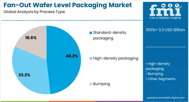
The standard-density packaging process type is projected to hold 48.2% of the fan-out wafer level packaging market revenue share in 2025, making it the leading process category. Its prominence is attributed to the balance it offers between cost-efficiency and performance, meeting the requirements of a broad range of semiconductor applications.
Standard-density packaging provides sufficient input/output density to support many consumer electronics devices without incurring the higher costs and complexities associated with ultra-high-density alternatives. The manufacturing processes for standard-density packaging are mature, enabling scalability and faster time to market, which are critical for fast-evolving end-use sectors.
Additionally, standard-density solutions enable flexibility in design and integration, supporting product customization and quicker adoption across diverse applications. The segment benefits from ongoing improvements in materials and process optimization, which further enhance reliability and electrical performance while maintaining competitive pricing.
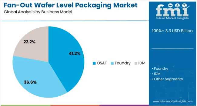
The outsourced semiconductor assembly and test (OSAT) business model is expected to account for 41.2% of the fan-out wafer level packaging market revenue share in 2025, emerging as the dominant model. The growth of OSAT providers is driven by increasing semiconductor manufacturing complexity, which has prompted many fabless and integrated device manufacturers to outsource assembly and testing to specialized partners.
OSAT companies offer advanced process expertise, flexible capacity, and investment in state-of-the-art equipment that many chipmakers find economically unfeasible to develop in-house. This model accelerates innovation cycles and reduces capital expenditure for semiconductor firms, supporting faster product introductions.
The expansion of OSAT capabilities in fan-out wafer level packaging, including support for high-volume production and customization, aligns with growing end-market demand. Furthermore, strategic collaborations and capacity expansions by OSAT providers globally are strengthening their market position and enabling more efficient supply chains for semiconductor packaging.
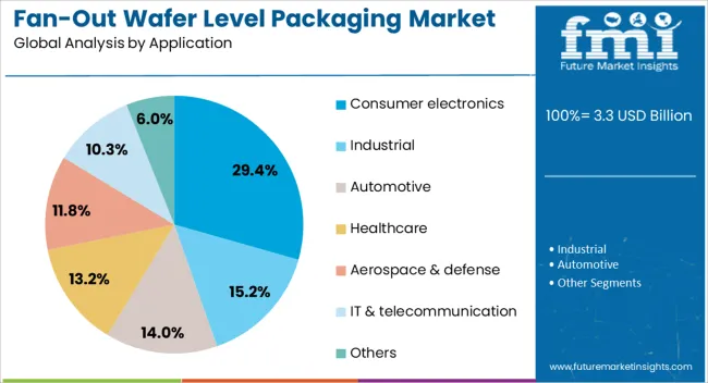
The consumer electronics application segment is anticipated to represent 29.4% of the fan-out wafer level packaging market revenue share in 2025, establishing itself as the leading end-use sector. The segment’s growth is being propelled by the continuous evolution and adoption of smartphones, tablets, wearable devices, and other connected consumer products requiring compact, high-performance packaging solutions.
Fan-out wafer level packaging enables smaller device footprints and enhanced electrical characteristics critical for consumer electronics, where size, weight, and battery life are key considerations. Rapid innovation cycles and demand for multi-functional devices with advanced features further increase reliance on flexible packaging technologies.
Additionally, growing penetration of smart home devices and IoT-enabled consumer products expands the addressable market for fan-out packaging. The segment is supported by strong consumer spending trends and ongoing technological upgrades, which collectively sustain high demand and encourage further development of tailored packaging solutions for this dynamic industry.
The fan-out wafer level packaging market is set to expand as device makers chase thinner profiles, higher I/O density, and better electrical/thermal behavior for compact electronics. Demand is reinforced by smartphones, wearables, automotive ADAS, RF front-ends, and AI/HPC accelerators that need low-inductance interconnects. Opportunities are opening around chiplets, system-in-package, and panel-level formats tied to localized manufacturing. Trends point to tighter RDL line/space, mold-first and RDL-first flows, and co-design with power delivery. Challenges include capex intensity, die-shift control, reliability proofs, and competition from 2.5D/FC-BGA routes.
Demand has been reinforced by application processors, RF front-ends, sensors, and power management ICs that benefit from fan-out wafer level packaging (FOWLP) through thinner stacks, short interconnect paths, and low parasitics. Smartphone and wearable platforms value compact form factors and better thermal spread, while automotive ADAS, radar, and domain controllers prioritize reliability and high I/O counts.
FOWLP (e.g., eWLB, InFO styles) wins where fine-pitch redistribution layer (RDL) density, warpage control, and package stiffness must be balanced without costly substrates. AI accelerators and edge inference modules are leaning toward fan-out for low-inductance power delivery and tight signal integrity in small footprints. Growth is also being driven by Wi-Fi 7 modules, mmWave 5G antenna-in-package, and IoT nodes requiring SiP integration. This mix places FOWLP as the practical choice when electrical performance, thinness, and volume economics intersect.
Opportunities are emerging as chiplet architectures and heterogeneous integration convert FOWLP into a high-value assembly platform. Multi-die system-in-package designs, power delivery overlays, and embedded passives inside mold compounds allow differentiated RF, compute, and mixed-signal modules. Panel-level packaging (PLP) is opening cost and throughput upsides, particularly for mid-size dies and RF components where substrate pricing is volatile. We see attractive openings in automotive-grade parts (AEC-Q qualifications), where corrosion resistance, thermal cycling endurance, and delamination control command premiums. Design-for-fan-out services, EDA co-design with RDL routing, known-good-die strategies, and turnkey OSAT partnerships create sticky revenue. Regional supply build-outs and government-backed fabs are expanding vendor lists, while co-packaged power stages for edge servers and base stations broaden scope. Providers that pair PLP capacity with chiplet-ready flows and fast qualification cycles will capture the highest-margin pipeline.
Trends are centering on tighter RDL (≤2–3 μm L/S), copper pillar micro-interconnects, and hybrid mold compounds to suppress warpage on large body sizes. Mold-first and RDL-first flows are being tuned for die shift control, with temporary bond/debond carriers, laser debond, and optimized cure profiles reducing stress. Antenna-in-package for mmWave, power SiP with thicker copper planes, and high-density fan-out for PMICs are gaining share as boards demand cleaner power/signal paths. Co-design for power distribution networks and thermal paths is becoming standard, alongside underfill and EMC choices that resist moisture ingress. Suppliers are also prioritizing low-alpha materials, fine-grain copper plating, and plasma treatments for adhesion. The decisive shift is toward manufacturable high-density fan-out that rivals interposer-based 2.5D for certain footprints, while panel-level rollouts push cost per I/O down without sacrificing reliability metrics.
Challenges include high capex for RDL lithography, plating, and molding lines, plus yield loss from die shift, bump/RDL defects, and voiding during reconstitution. Qualification cycles are lengthy: thermal cycling, temperature-humidity-bias, electromigration, and drop tests stretch program timelines, particularly for automotive and industrial electronics. Raw material swings in copper foil, photoresists, and mold compounds pressure margins, while tool availability for panel formats remains tight. Supply concentration in a handful of OSATs and foundry-affiliated houses creates allocation risk. Competition from flip-chip BGA with Ajinomoto-based substrates, 2.5D interposers, and advanced fan-in WLP can cap pricing power. Winners will be those who standardize design rules, automate warpage/die-shift metrology, and lock multi-sourcing for critical chemistries; otherwise, cost volatility and qualification bottlenecks will restrain broader adoption.
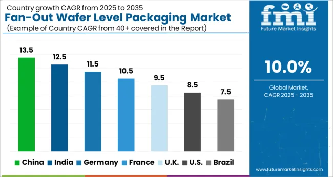
| Country | CAGR |
|---|---|
| China | 13.5% |
| India | 12.5% |
| Germany | 11.5% |
| France | 10.5% |
| UK | 9.5% |
| USA | 8.5% |
| Brazil | 7.5% |
The global fan-out wafer level packaging (FOWLP) market is projected to grow at a CAGR of 10% from 2025 to 2035. China is estimated at 13.5%, India at 12.5%, and France at 10.5%, while the UK and US are expected at 9.5% and 8.5%, respectively. Demand is being propelled by chiplet architectures, antenna-in-package (AiP) for 5G/mmWave, power-efficient mobile SoCs, and heterogeneous integration for AI and automotive control units. Cost advantages in redistribution layers (RDL), thinner profiles, and improved thermals are reinforcing migration from wire-bond and flip-chip in several consumer and RF front-end lines. Europe is set to emphasize reliability, warpage control, and SiP qualification, while Asia is positioned to scale capacity and panel-level pilots. The US outlook appears steady, led by AI accelerators and defense electronics. This report includes insights on 40+ countries; the top markets are highlighted for reference.
The fan-out wafer level packaging market in China is projected to expand at a CAGR of 13.5%. Growth is being supported by mobile application processors, RF front-end modules, and power management ICs shifting toward thin-profile, high-I/O formats. Local OSAT capacity for multi-die RDL, fine-line copper, and mold-underfill control has been expanded, while yield learning on large body sizes has improved cost curves. AiP for 5G customer premises equipment and smartphones is being prioritized, with form-factor gains valued by OEMs. Migration toward fan-out panel-level packaging (FOPLP) is under assessment to reduce the cost per unit area. With domestic design houses increasing tape-outs for consumer and industrial edge compute, China is expected to cement a leading share in volume programs across consumer, RF, and power categories.
The fan-out wafer level packaging market in India is expected to grow at a CAGR of 12.5%. Momentum is being created by ATMP expansions, design-services hubs, and partnerships with global OSATs that route advanced packages to regional lines. Early adoption is centered on IoT radios, wearables, and entry automotive ECUs where compact footprints and shorter interconnects are valued. Government production-linked incentives and electronics clusters are encouraging local qualification of RDL processes and reliability testing. Universities and labs are being engaged for package design, thermal modeling, and board-level drop assessments, improving time-to-qualification for domestic brands. As EMS providers scale, demand for SiP with discrete passives embedded around fan-out dies is set to rise, positioning India as a fast-growing destination for cost-sensitive FOWLP programs.
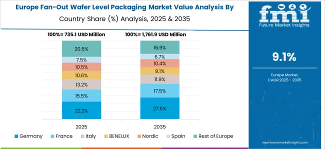
The fan-out wafer level packaging market in France is projected to expand at a CAGR of 10.5%. Demand is being shaped by automotive powertrains, industrial control, avionics, and secure payments, where thin profiles and low parasitics are valued. R&D centers and leading device makers are prioritizing reliability screens, high-temperature storage, temperature cycling, and moisture sensitivity, alongside warpage mitigation for larger body formats. Power management ICs and sensor hubs are migrating to fan-out to reduce package inductance and improve thermal paths without heat spreaders. European supply chains are favoring traceable materials and lot-level analytics, strengthening audits for high-reliability lines. With strong emphasis on SiP qualification and RF modules for V2X and smart mobility, France is poised to scale mid-volume, high-margin programs in FOWLP and panel-ready derivatives.
The fan-out wafer level packaging market in the UK is forecast to grow at a CAGR of 9.5%. Activity is being concentrated around RF, photonics, and compound-semiconductor ecosystems serving aerospace, defense, and telecom. Pilot lines emphasize fine-pitch RDL, die-thinning, and co-design with antenna structures for beamforming modules. University-industry collaborations are advancing metrology for die shift, voiding, and copper trace integrity, raising first-pass yield on complex packages. With domestic volume limited, high-value prototypes and pre-production lots are being routed to partner OSATs after local design and reliability sign-off. As chiplet architectures gain traction, UK teams are expected to use fan-out as a routing and interposer-light alternative for small tiles. This niche orientation supports premium engagements rather than mass consumer runs.
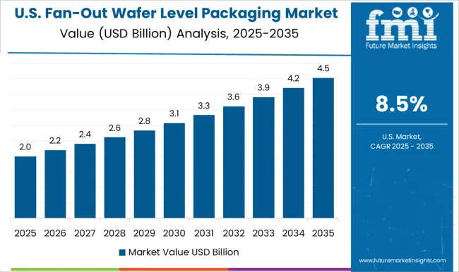
The fan-out wafer level packaging market in the US is projected to grow at a CAGR of 8.5%. Uptake is being led by AI accelerators, networking ASICs, and mmWave front-ends that benefit from short interconnects, reduced parasitics, and improved power integrity. Advanced packaging initiatives are encouraging domestic lines for RDL, mold, and debond, while collaborations with fabless leaders align package layouts with chiplet roadmaps. Data-center programs are examining fan-out as a complementary path to 2.5D, especially where interposer costs are restrictive. Automotive ADAS and radar modules are adding steady demand for AiP and compact SiP. With reliability expectations set high, process windows for large-body fan-out are being tightened to contain warpage and delamination risks, positioning US suppliers for selective, high-value ramps.
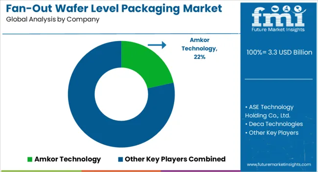
Market rivalry is shaped by packaging type, integration capability, thermal and electrical performance, cost efficiency, and production scalability. Companies differentiate through advanced packaging technologies, proprietary solutions, and strong R&D capabilities that enhance device performance and reduce form factor.
Key players such as TSMC, ASE Technology, Amkor Technology, JCET Group, Samsung Electro-Mechanics, Powertech Technology, and Nepes Corporation dominate the market with high-performance, reliable, and technologically advanced FOWLP solutions. Strategic collaborations between semiconductor manufacturers and packaging service providers are leveraged to expand capabilities and accelerate adoption. Regional expansion, particularly in Asia-Pacific and Japan, supports increased production capacity and addresses global demand.
Emerging players compete by offering cost-effective, specialized, and flexible packaging solutions. The market is moderately consolidated, with leading companies focusing on technological innovation, material optimization, and long-term service agreements to maintain market share and meet the evolving needs of the electronics industry.
| Item | Value |
|---|---|
| Quantitative Units | USD 3.3 Billion |
| Process Type | Standard-density packaging, High-density packaging, and Bumping |
| Business Model | OSAT, Foundry, and IDM |
| Application | Consumer electronics, Industrial, Automotive, Healthcare, Aerospace & defense, IT & telecommunication, and Others |
| Regions Covered | North America, Europe, Asia-Pacific, Latin America, Middle East & Africa |
| Country Covered | United States, Canada, Germany, France, United Kingdom, China, Japan, India, Brazil, South Africa |
| Key Companies Profiled | Amkor Technology, ASE Technology Holding Co., Ltd., Deca Technologies, GlobalFoundries Inc., JCET Group Co., Ltd., Nepes Corporation, Powertech Technology Inc., and Siliconware Precision Industries Co., Ltd. |
| Additional Attributes | Dollar sales by package type (core, high density, panel level), Dollar sales by application (AP/SoC, RF, power management, memory), Trends in heterogeneous integration and chiplet architectures, Role in enabling high I/O and thermal performance, Growth driven by 5G, AI accelerators, automotive electronics, Regional manufacturing across Asia Pacific, North America, Europe. |
The global fan-out wafer level packaging market is estimated to be valued at USD 3.3 billion in 2025.
The market size for the fan-out wafer level packaging market is projected to reach USD 8.6 billion by 2035.
The fan-out wafer level packaging market is expected to grow at a 10.0% CAGR between 2025 and 2035.
The key product types in fan-out wafer level packaging market are standard-density packaging, high-density packaging and bumping.
In terms of business model, osat segment to command 41.2% share in the fan-out wafer level packaging market in 2025.


Full Research Suite comprises of:
Market outlook & trends analysis
Interviews & case studies
Strategic recommendations
Vendor profiles & capabilities analysis
5-year forecasts
8 regions and 60+ country-level data splits
Market segment data splits
12 months of continuous data updates
DELIVERED AS:
PDF EXCEL ONLINE
Wafer Batch Aligner Market Size and Share Forecast Outlook 2025 to 2035
Wafer Manufacturing Equipment Market Size and Share Forecast Outlook 2025 to 2035
Wafer Inspection Market Size and Share Forecast Outlook 2025 to 2035
Wafer Cleaning Equipment Market Growth - Trends & Forecast 2025 to 2035
Wafer Testing Service Market Growth – Trends & Forecast 2024-2034
Wafer Level Packaging Market Size and Share Forecast Outlook 2025 to 2035
InP Wafer Market Size and Share Forecast Outlook 2025 to 2035
Thin Wafer Processing and Dicing Equipment Market Size and Share Forecast Outlook 2025 to 2035
Thin Wafers Market Analysis - Size, Demand & Growth 2025 to 2035
Manual Wafer Aligner Market Analysis - Size, Share, and Forecast Outlook 2025 to 2035
Silicon Epi Wafer Market Size and Share Forecast Outlook 2025 to 2035
Solar Silicon Wafer Market Size and Share Forecast Outlook 2025 to 2035
Semiconductor Wafer Market – Forecast through 2025 to 2035
Solar Photovoltaic Wafer Market
Optical Grade Lithium Tantalate Wafers Market Size and Share Forecast Outlook 2025 to 2035
Packaging Supply Market Size and Share Forecast Outlook 2025 to 2035
Packaging Testing Services Market Size and Share Forecast Outlook 2025 to 2035
Packaging Tubes Market Size and Share Forecast Outlook 2025 to 2035
Packaging Jar Market Forecast and Outlook 2025 to 2035
Packaging Barrier Film Market Size and Share Forecast Outlook 2025 to 2035

Thank you!
You will receive an email from our Business Development Manager. Please be sure to check your SPAM/JUNK folder too.
Chat With
MaRIA