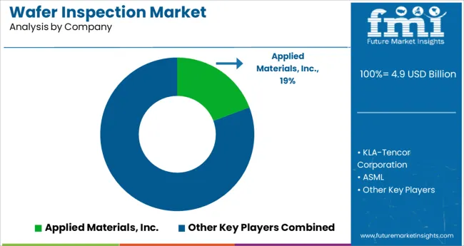
The Wafer Inspection Market is estimated to be valued at USD 4.9 billion in 2025 and is projected to reach USD 13.3 billion by 2035, registering a compound annual growth rate (CAGR) of 10.6% over the forecast period.
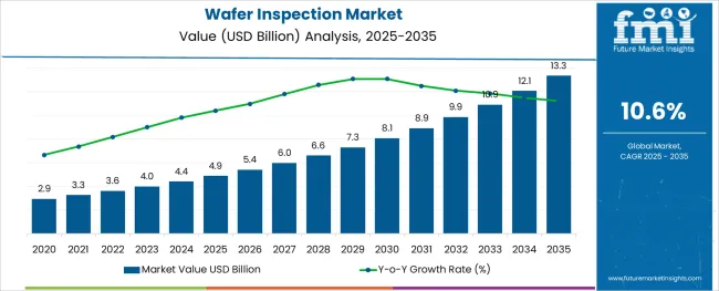
The wafer inspection market is experiencing robust growth, fueled by the rising complexity of semiconductor node architectures and the demand for zero-defect manufacturing environments. As chipmakers transition toward sub-5nm and advanced packaging technologies, the requirement for ultra-precise inspection tools has intensified.
Optical and e-beam technologies are being adopted to meet yield targets and minimize line failures through early-stage defect identification. Equipment manufacturers are integrating AI-based analytics to enhance sensitivity and reduce false positives, while fab operators are investing in real-time monitoring and defect classification tools to reduce downtime and operational inefficiencies.
With semiconductor fabs expanding globally, particularly across Asia-Pacific and North America, demand for high-throughput, inline inspection systems is accelerating. Future growth is expected to be supported by increased investment in foundry capacity, greater reliance on heterogeneous integration, and the integration of defect data into predictive process control systems that ensure quality and yield continuit.
The market is segmented by Technology and Defect Type and region. By Technology, the market is divided into Optical detection technology and E-beam detection technology. In terms of Defect Type, the market is classified into Random defects detection and Systematic defects detection. Regionally, the market is classified into North America, Latin America, Western Europe, Eastern Europe, Balkan & Baltic Countries, Russia & Belarus, Central Asia, East Asia, South Asia & Pacific, and the Middle East & Africa.
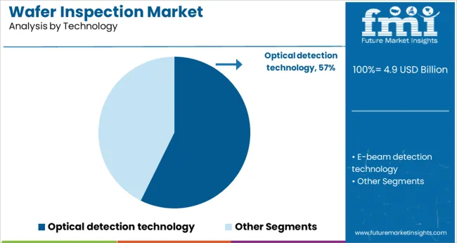
The optical detection technology segment is projected to capture 57.3% of the total revenue in 2025, making it the leading technology in the wafer inspection market. This segment’s dominance is supported by its superior throughput, cost-efficiency, and non-invasive nature, making it ideal for inline inspection across various process nodes.
Optical systems are capable of detecting a wide range of surface-level defects such as particles, pattern deformation, and bridging, which are critical during front-end semiconductor manufacturing. Advancements in high-resolution imaging, deep learning algorithms, and adaptive optics have enhanced defect detection accuracy without compromising inspection speed.
Optical tools have also gained preference due to their relatively lower operating and maintenance costs compared to electron-based systems. Their scalability across both mature and advanced technology nodes has further reinforced their widespread adoption, particularly in high-volume manufacturing environments where time-sensitive defect identification is essential for maintaining yields.
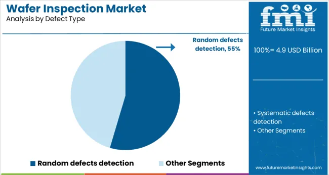
Random defects detection is anticipated to account for 54.6% of the total revenue share in 2025 within the defect type category, solidifying its position as the dominant inspection focus. The prominence of this segment is driven by the critical role random defects play in yield loss and reliability failures across shrinking semiconductor nodes.
As device geometries become more compact and multilayered, random defectivity introduced during etching, deposition, and lithography steps becomes increasingly unpredictable and difficult to isolate. Detection tools have evolved to identify sub-nanometer anomalies using AI-based classification and advanced imaging techniques.
Semiconductor manufacturers are prioritizing inspection systems that can effectively capture stochastic defects at early process stages, reducing the risk of costly rework or wafer scrap. The unpredictable nature of these defects demands continuous inspection and real-time analytics, making this segment a focal point in the push toward fully automated and predictive semiconductor manufacturing lines.
Increased demand for Integrated Circuits
There has been a massive increase in the growth of the semiconductor industry. Integrated circuits are a significant part of the semiconductors because of which there is a proportional increase in the application of Integrated Circuits. Moreover, in order to keep a check on the condition of the substrates which are present below the IC, Wafer inspections are employed.
This is well expected to increase the sales of wafer inspections.
Rise in the usage of electronic devices
With the evolution of the electronic industry, it is quite clear that almost every aspect of electronic devices has undergone a massive transformation. It can be in terms of size of the device, performance of device etc. It is relevant to note here that these wafer inspections are used before such circuits are embedded in these devices.
Consistent evolution of telecom sector
The most trending discussion point in the present telecom sector is the rise of 5G. However, there are parts of the world where the testing and implementation of 6G as well has begun. All these generations of telecommunication technology can only work if the towers are installed at the right places.
Moreover, for the immaculate operation of these towers, there are a number of semiconductors which are put into place, both at the site and in the control stations. This is expected to massively influence the demand for wafer inspection.
Ability to detect even minutest of defects
Working inside a semiconductor would mean dealing with extremely small defects which in the range of nanometres. The best part about making use of the wafer inspections is that they are able to detect scratches, wafer edge flaws, spin defects etc. with a high precision.
High Cost
Though the application of Wafer inspections has a lot of benefits, the cost associated with its usage is quite high. Because of this, only those players with high purchasing power can afford this device.
This might have a level on influence on the sales of wafer inspection.
Shrinking size of circuits
Despite the ability to work in the defects which are of nanometre range, the Wafer inspection may not act effectively on the upcoming circuits. The reason being that the focus of manufacturers mainly lies to further reduce the size of these circuits. These present a potential challenge in front of the wafer integration system market.
Growth of IT, IoT, and E-Commerce
The IT, IoT, and eCommerce are all set to experience enormous growth in the coming years. Moreover, these industries extensively make use of wireless technology. The application of wireless technology is possible with the usage of IC’s and semiconductors.
This presents a galaxy of opportunity in front of the wafer inspection market.
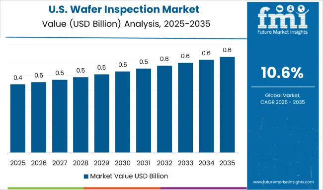
The North American Wafer inspection market currently occupies 29.4% of the market share, and during the period 2025 to 2035, the market is expected to rise further in the region.
Massive development in electronics industry, coupled with the increasing usage of electronic devices like TV, smartphones etc., are expected to increase the demand for Wafer inspection in the region. Moreover, even the companies present in this region are willing to spend on the application of Wafer inspections.
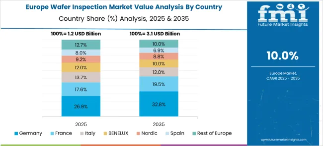
The European wafer inspection market currently has a market share of 26.5%, and during the forecast period, the market is expected to grow.
The reason remains the same as in the case of North America, i.e., development in electronics industry and willingness of the companies to spend on wafer inspection. Moreover, the manufacturers in this region are very particular about the quality and performance of integrated circuits. This is expected to drive the sales of wafer inspection.
The growth of the semiconductor industry has presented a doorway of opportunities for the start-ups.
The start-ups are mainly focusing at working on the miniaturised circuits. They are effectively looking for ways to rectify the defects which are beyond nanometre range to work in tandem with the current requirements of the ICs.
Saccade develops solutions for dimensional and targeted inspection of precise manufacturing. The firm makes use of MEMS-based laser inspection system. This ensures anti-defect manufacturing while reducing costs.
With a view to widen their presence, the key players in wafer inspection market are looking to expand their operations across countries. This will enable the host country by purchasing the device at a relatively lower cost, and even the quality will not be compromised.
| Report Attribute | Details |
|---|---|
| Growth Rate | CAGR of 10.6% from 2025 to 2035 |
| Base Year for Estimation | 2025 |
| Historical Data | 2020 to 2024 |
| Forecast Period | 2025 to 2035 |
| Quantitative Units | Revenue in USD Million and CAGR from 2025-2035 |
| Report Coverage | Revenue Forecast, Volume Forecast, Company Ranking, Competitive Landscape, Growth Factors, Trends and Pricing Analysis |
| Segments Covered | Technology, Defect Type, Region |
| Regions Covered | North America; Latin America; Asia Pacific; MEA; Europe |
| Key Countries Profiled | The USA, Canada, Brazil, Argentina, Germany, The UK, France, Spain, Italy, Nordics, BENELUX, Australia & New Zealand, China, India, GCC, South Africa |
| Key Companies Profiled | Applied Materials, Inc.; KLA-Tencor Corporation; ASML; Hermes Microvision, Inc.; Hitachi High-Technologies Corporation; Lam Research Corporation; Nanda Technologies GmBH; NXP Semiconductors; Taiwan Semiconductor Manufacturing Company Limited; Synopsys |
| Customization | Available Upon Request |
How big is the wafer inspection market in 2025?
The global wafer inspection market is estimated to be valued at USD 4.9 billion in 2025.
What will be the market size for the wafer inspection market in 2035?
It is projected to reach USD 13.3 billion by 2035.
How much will be the CAGR of the wafer inspection market between 2025 and 2035?
The market is expected to grow at a 10.6% CAGR between 2025 and 2035.
What are the key product types in the wafer inspection market?
The key product types are optical detection technology and e-beam detection technology.
Which random defects detection segment is expected to dominate the wafer inspection market in 2025?
random defects detection segment is expected to dominate with a 54.6% industry share in 2025.
Full Research Suite comprises of:
Market outlook & trends analysis
Interviews & case studies
Strategic recommendations
Vendor profiles & capabilities analysis
5-year forecasts
8 regions and 60+ country-level data splits
Market segment data splits
12 months of continuous data updates
DELIVERED AS:
PDF EXCEL ONLINE

Thank you!
You will receive an email from our Business Development Manager. Please be sure to check your SPAM/JUNK folder too.