The wafer batch aligner industry stands at the threshold of a decade-long expansion trajectory that promises to reshape semiconductor manufacturing and precision alignment technology. The market's journey from USD 418.2 million in 2025 to USD 748.9 million by 2035 represents substantial growth, demonstrating the accelerating adoption of advanced semiconductor fabrication equipment and automated alignment systems across electronics manufacturing, automotive semiconductors, and advanced chip production sectors.
The first half of the decade (2025-2030) will see the market increase from USD 418.2 million to approximately USD 550.8 million, adding USD 132.6 million in value, which constitutes 40% of the total forecasted growth period. This phase will be characterized by the rapid adoption of automated wafer batch aligner systems, driven by increasing demand for semiconductors and modernization programs in the global manufacturing sector. Advanced precision capabilities and automated handling features will become standard expectations rather than premium options.
The latter half (2030-2035) will witness sustained growth from USD 550.8 million to USD 748.9 million, representing an addition of USD 198.1 million or 60% of the decade's expansion. This period will be defined by mass market penetration of next-generation alignment systems, integration with comprehensive semiconductor manufacturing platforms, and seamless compatibility with existing fab infrastructure. The market trajectory signals fundamental shifts in how semiconductor manufacturers approach wafer processing and batch handling, with participants positioned to benefit from sustained demand across multiple application segments.
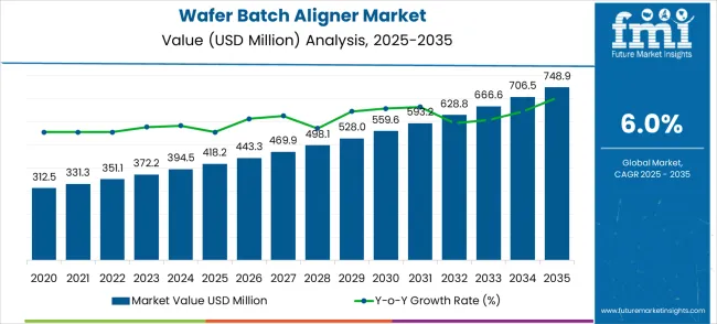
The Wafer Batch Aligner market demonstrates distinct growth phases with varying market characteristics and competitive dynamics. Between 2025 and 2030, the market progresses through its technology adoption phase, expanding from USD 418.2 million to USD 550.8 million with steady annual increments averaging 5.7% growth. This period showcases the transition from basic manual alignment systems to advanced automated platforms with enhanced precision capabilities and integrated process control systems becoming mainstream features.
The 2025-2030 phase adds USD 132.6 million to market value, representing 40% of total decade expansion. Market maturation factors include standardization of automation protocols, declining component costs for precision alignment systems, and increasing semiconductor manufacturer awareness of automated batch processing benefits reaching 90-95% efficiency improvements in wafer handling applications. Competitive landscape evolution during this period features established semiconductor equipment manufacturers like Emu Technologies and SPS-International expanding their wafer batch aligner portfolios while new entrants focus on compact designs and enhanced throughput capabilities.
From 2030 to 2035, market dynamics shift toward advanced integration and multi-platform deployment, with growth accelerating from USD 550.8 million to USD 748.9 million, adding USD 198.1 million or 60% of total expansion. This phase transition logic centers on next-generation automated systems, integration with Industry 4.0 manufacturing networks, and deployment across diverse semiconductor fabrication scenarios, becoming standard rather than specialized applications. The competitive environment matures with focus shifting from basic alignment capability to comprehensive wafer handling systems and integration with fab-wide automation and process control platforms.
| Metric | Value |
|---|---|
| $ Market Value (2025) → | USD 418.2 million |
| $ Market Forecast (2035) ↑ | USD 748.9 million |
| # Growth Rate ★ | 6.0% CAGR |
| Leading Technology → | Automated Type |
| Primary Application → | Wafer Segment |
The market demonstrates strong fundamentals with automated operation mode systems capturing a dominant 68.5% share through advanced precision and high-throughput batch processing capabilities. Wafer applications drive primary demand with 72.3% market share, supported by increasing semiconductor production and advanced chip manufacturing requirements. Geographic expansion remains concentrated in developed markets with established semiconductor infrastructure, while emerging economies show accelerating adoption rates driven by electronics manufacturing growth and rising fab investments.
Market expansion rests on three fundamental shifts driving adoption across semiconductor and electronics manufacturing sectors.
However, growth faces headwinds from technical complexity challenges that vary across different substrate types and processing requirements, which may limit operational flexibility in certain manufacturing environments. Cost considerations also persist regarding initial capital investment and integration expenses that may reduce system adoption rates in price-sensitive market segments that prioritize immediate cost savings over long-term automation benefits.
The wafer batch aligner market presents significant growth opportunities as global semiconductor manufacturing paradigms shift toward automated precision alignment solutions and Industry 4.0 integration accelerates worldwide. With the market projected to expand from USD 418.2 million in 2025 to USD 748.9 million by 2035 at a 6.0% CAGR, semiconductor equipment manufacturers and technology providers are positioned to capitalize on structural demand from chip fabrication facilities, electronics manufacturers, and research institutions requiring precise wafer handling and alignment capabilities.
The convergence of semiconductor manufacturing modernization programs, increasing chip complexity requirements, and automation emphasis on precision processing creates sustained market expansion opportunities. Geographic growth differentials are particularly pronounced in China (8.1% CAGR) and India (7.5% CAGR), where rapid semiconductor development and manufacturing infrastructure investments drive substantial demand. Technology advancement pathways around automation, precision enhancement, and process integration offer differentiation opportunities, while specialized applications across wafer processing, compound semiconductor manufacturing, and research facilities provide diverse revenue streams.
Automated system dominance and wafer application leadership indicate established foundations for strategic expansion, while SiC & GaN substrate applications represent emerging growth vectors. Semiconductor manufacturing investments globally support sustained procurement, while advanced packaging and specialty substrate requirements drive operational deployment.
Primary Market Structure: The market segments by operation mode into Automated and Manual categories, representing the evolution from traditional operator-dependent systems to advanced automated platforms for comprehensive precision handling and batch processing efficiency.
Secondary Breakdown: Application segmentation divides the market into Wafer and SiC & GaN Substrate sectors, reflecting distinct requirements for conventional silicon processing, compound semiconductor manufacturing, and specialty substrate handling applications.
Regional Distribution: Geographic classification covers Asia Pacific, North America, Europe, Latin America, and the Middle East & Africa, with established semiconductor manufacturing regions leading adoption while emerging economies show accelerating growth patterns driven by electronics manufacturing development programs.
The segmentation structure reveals technology progression from manual alignment systems toward fully automated platforms with enhanced precision and throughput capabilities, while application diversity spans from traditional silicon wafer processing to emerging compound semiconductor manufacturing requiring specialized handling solutions for advanced material properties.
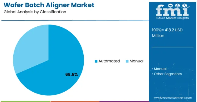
Market Position: Automated operation mode systems command the leading position in the wafer batch aligner market with 68.5% market share through advanced precision features, including robotic handling capabilities, computer-controlled positioning, and integrated process monitoring that enable semiconductor manufacturers to achieve consistent alignment accuracy across high-volume batch processing operations.
Value Drivers: The segment benefits from semiconductor industry preference for automated systems that provide superior repeatability and contamination control without requiring skilled operator intervention for each alignment cycle. Automated design features enable deployment in cleanroom environments, high-throughput manufacturing, and 24/7 production operations where consistency and reliability represent critical operational requirements for advanced chip manufacturing and substrate processing applications.
Competitive Advantages: Automated systems differentiate through intelligent control algorithms, adaptive positioning capabilities, and integration with fab-wide automation networks that enhance manufacturing efficiency while maintaining precision tolerances suitable for sub-micron semiconductor processing requirements and advanced packaging operations.
Key market characteristics:
The Manual operation mode segment maintains 31.5% market share, primarily serving research applications, low-volume production, and specialized processing requirements where operational flexibility and cost considerations outweigh automation benefits in specific manufacturing scenarios.
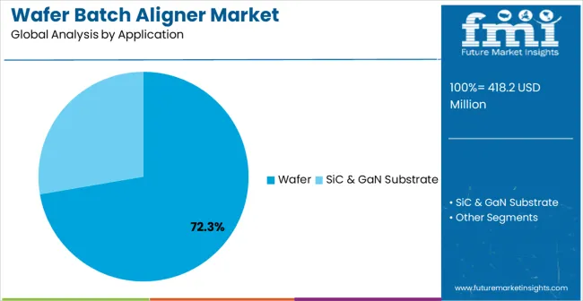
Market Context: Wafer applications dominate the wafer batch aligner market with 72.3% market share due to widespread silicon semiconductor manufacturing and increasing focus on advanced chip production, packaging operations, and substrate processing applications that require precise alignment control for maintaining device performance and manufacturing yield optimization.
Appeal Factors: Wafer processing customers prioritize alignment accuracy, throughput optimization, and integration with existing semiconductor fabrication equipment that enables coordinated processing across multiple manufacturing stages. The segment benefits from substantial semiconductor industry investments and technology advancement programs that emphasize automated handling solutions for conventional silicon wafer processing in logic, memory, and mixed-signal device manufacturing applications.
Growth Drivers: Semiconductor industry expansion incorporates wafer batch aligners as essential equipment for advanced node processing and packaging operations, while increasing chip complexity and miniaturization drive demand for precision alignment capabilities that maintain device specifications and manufacturing quality standards. Advanced packaging trends, including 3D integration and system-in-package solutions, create additional alignment requirements for specialized wafer handling and substrate preparation processes.
Market Challenges: Substrate handling complexity and diverse wafer specifications may require customized alignment solutions that increase system costs and reduce standardization benefits across different semiconductor manufacturing applications and process requirements.
Application dynamics include:
The SiC & GaN Substrate segment holds 27.7% market share, representing emerging opportunities in compound semiconductor manufacturing for power electronics, RF applications, and specialty device production where unique material properties require specialized alignment solutions and handling protocols.
Growth Accelerators: Semiconductor manufacturing modernization drives primary adoption as wafer batch aligner systems provide automated precision positioning that enables consistent wafer handling with sub-micron accuracy, supporting advanced node processing and compound semiconductor manufacturing that require precise alignment tolerances. Manufacturing automation demand accelerates market expansion as semiconductor fabs seek efficient batch processing tools that minimize human intervention while maintaining contamination control and yield optimization during critical wafer handling operations and substrate preparation processes. Electronics industry growth creates sustained demand for automated handling equipment that complements advanced manufacturing systems and provides operational flexibility in complex fab environments where precision and repeatability represent critical manufacturing requirements.
Industry 4.0 integration trends further amplify adoption as manufacturers implement smart factory concepts requiring automated equipment with process monitoring capabilities, real-time data collection, and integration with manufacturing execution systems that optimize production workflow and enable predictive maintenance scheduling. Advanced packaging requirements drive specialized alignment system demand as semiconductor manufacturers adopt new packaging technologies including 3D integration, system-in-package solutions, and heterogeneous integration approaches that necessitate precise wafer positioning and substrate handling capabilities beyond traditional applications.
Compound semiconductor market expansion, particularly in SiC and GaN substrate processing, creates specialized alignment requirements due to unique material properties and processing challenges that demand customized handling solutions with enhanced precision control and contamination prevention features. Research and development activity acceleration in semiconductor technology drives demand for flexible alignment systems capable of handling diverse substrate types and experimental processing requirements that support next-generation chip development and advanced material research applications.
Growth Inhibitors: Capital investment barriers persist as wafer batch aligner systems require substantial initial investment costs ranging from hundreds of thousands to millions of dollars per unit, which may limit adoption among smaller semiconductor manufacturers and research facilities operating under constrained budgets or uncertain return on investment scenarios. Technical complexity challenges create integration difficulties when incorporating new alignment systems into existing fab infrastructure, particularly in older facilities where legacy equipment compatibility and process modification requirements can result in extended implementation timelines and additional engineering costs.
Substrate compatibility limitations affect market penetration as specialized substrates including compound semiconductors, advanced packaging materials, and experimental wafers may require customized alignment solutions that increase system costs and reduce standardization benefits. Market fragmentation across diverse semiconductor applications creates compatibility concerns between different alignment system manufacturers and existing process equipment, potentially limiting supplier selection and increasing procurement complexity for fab operators managing multiple equipment vendor relationships.
Supply chain vulnerabilities in precision components and advanced automation systems can impact delivery schedules and system availability, particularly during periods of high semiconductor equipment demand when component shortages and extended lead times affect customer deployment plans and facility expansion timelines.
Market Evolution Patterns: Technology adoption accelerates in advanced semiconductor manufacturing facilities where precision alignment justifies system costs, with geographic concentration in major semiconductor regions transitioning toward mainstream adoption in emerging manufacturing hubs driven by electronics production growth and fab establishment programs. Automation sophistication increases as alignment systems incorporate artificial intelligence, machine learning algorithms, and advanced sensor technologies that enhance precision control and enable adaptive processing capabilities for diverse substrate handling requirements.
Market consolidation trends emerge as larger semiconductor equipment manufacturers acquire specialized alignment system companies to expand technology portfolios and provide comprehensive automation solutions that address complete wafer handling workflows. The market could face disruption if alternative alignment technologies or revolutionary substrate handling approaches significantly change semiconductor manufacturing processes or eliminate traditional batch processing requirements in advanced chip production environments.
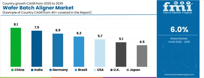
The wafer batch aligner market demonstrates varied regional dynamics with Growth Leaders including China (8.1% CAGR) and India (7.5% CAGR) driving expansion through semiconductor manufacturing development and electronics production infrastructure growth. Steady Performers encompass Germany (6.9% CAGR), Brazil (6.3% CAGR), and the U.S. (5.7% CAGR), benefiting from established semiconductor industries and advanced manufacturing technology adoption. Mature Markets feature the U.K. (5.1% CAGR) and Japan (4.5% CAGR), where specialized semiconductor applications and precision manufacturing integration support consistent growth patterns.
| Country | CAGR (2025-2035) |
|---|---|
| China | 8.1% |
| India | 7.5% |
| Germany | 6.9% |
| Brazil | 6.3% |
| U.S. | 5.7% |
| U.K. | 5.1% |
| Japan | 4.5% |
Regional synthesis reveals Asia-Pacific markets leading growth through semiconductor manufacturing expansion and electronics production infrastructure development, while European countries maintain steady expansion supported by advanced manufacturing technology and research facility investments. North American markets show moderate growth driven by semiconductor innovation and advanced packaging applications.
The report covers an in-depth analysis of 40+ countries; seven top-performing countries are highlighted below.
China establishes market leadership through aggressive semiconductor manufacturing development programs and comprehensive electronics production infrastructure expansion, integrating advanced wafer batch aligner systems as standard components in fab automation and precision substrate handling applications. The country's 8.1% CAGR through 2035 reflects government initiatives promoting domestic semiconductor capability and electronics manufacturing competitiveness that mandate automated handling systems in manufacturing facilities and research installations. Growth concentrates in major semiconductor clusters, including Shanghai, Shenzhen, and Beijing, where technology development showcases integrated wafer batch aligner systems that appeal to domestic manufacturers seeking automated precision handling capabilities and advanced packaging applications.
Chinese manufacturers are developing cost-effective wafer batch aligner solutions that combine domestic production advantages with advanced automation features, including precision positioning systems and integrated process control capabilities. Distribution channels through state electronics programs and manufacturing equipment suppliers expand market access, while government funding for semiconductor technology development supports adoption across diverse manufacturing and research segments.
Strategic Market Indicators:
In Bangalore, Chennai, and Hyderabad, semiconductor facilities and electronics manufacturers are implementing advanced wafer batch aligner systems as standard equipment for precision handling operations and substrate processing applications, driven by increasing electronics production and government programs that emphasize manufacturing competitiveness and technology advancement capabilities. The market is projected to demonstrate a 7.5% CAGR through 2035, supported by government electronics manufacturing initiatives and semiconductor development programs that promote automated handling equipment for domestic facilities and international partnership projects. Indian electronics companies are adopting wafer batch aligner systems that provide efficient substrate processing capabilities and automated handling features, particularly appealing in technology centers where precision manufacturing represents critical operational requirements for export competitiveness.
Market expansion benefits from growing electronics manufacturing capabilities and international technology partnerships that enable domestic production of advanced handling systems for semiconductor and electronics applications. Technology adoption follows patterns established in manufacturing automation, where precision control and reliability drive procurement decisions and operational deployment strategies.
Market Intelligence Brief:
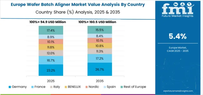
Germany's advanced manufacturing technology market demonstrates sophisticated wafer batch aligner deployment with documented operational effectiveness in semiconductor research facilities and precision manufacturing applications through integration with existing automation systems and quality control infrastructure. The country leverages engineering expertise in precision machinery and automation systems integration to maintain a 6.9% CAGR through 2035. Technology centers, including Dresden, Munich, and Stuttgart, showcase premium installations where wafer batch aligners integrate with comprehensive manufacturing platforms and research equipment to optimize substrate handling effectiveness and process precision capabilities.
German equipment manufacturers prioritize system precision and industry compatibility in wafer batch aligner development, creating demand for premium systems with advanced features, including environmental control and integration with research facility infrastructure. The market benefits from established manufacturing technology leadership and willingness to invest in advanced automation technologies that provide long-term operational benefits and support research excellence requirements.
Market Intelligence Brief:
Brazil's market expansion benefits from diverse electronics manufacturing demand, including semiconductor assembly in São Paulo and Campinas, technology development equipment upgrades, and government electronics programs that increasingly incorporate automated handling solutions for manufacturing competitiveness applications. The country maintains a 6.3% CAGR through 2035, driven by rising electronics production and increasing awareness of wafer batch aligner technology benefits, including automated processing and quality improvement capabilities for domestic manufacturing operations.
Market dynamics focus on cost-effective wafer batch aligner solutions that balance advanced handling features with affordability considerations important to Brazilian electronics manufacturers. Growing technology sector development creates sustained demand for precision handling systems in manufacturing infrastructure and research facility modernization projects.
Strategic Market Considerations:
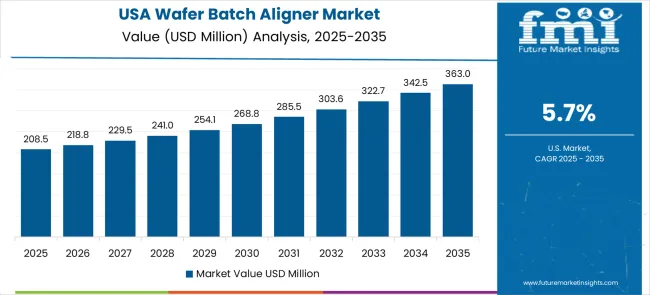
The U.S. market emphasizes advanced wafer batch aligner features, including precision automation systems and integration with comprehensive semiconductor manufacturing platforms that manage substrate handling, process control, and quality assurance applications through unified automation systems. The country is projected to show a 5.7% CAGR through 2035, driven by semiconductor industry modernization under manufacturing equipment upgrades and research facility demand for reliable automated handling systems with advanced positioning capabilities. American semiconductor manufacturers prioritize operational effectiveness with wafer batch aligners delivering consistent substrate positioning through advanced control algorithms and environmental adaptation capabilities for diverse processing requirements.
Technology deployment channels include major semiconductor equipment suppliers, specialized automation system providers, and research facility procurement programs that support professional installation for complex manufacturing applications. Semiconductor industry integration capabilities with established manufacturing systems expand market appeal across diverse operational requirements seeking precision and reliability benefits in advanced chip production environments.
Performance Metrics:
In Cambridge, Edinburgh, and other research centers, British semiconductor research facilities and electronics manufacturers are implementing advanced wafer batch aligner systems to enhance precision handling capabilities and support compound semiconductor development that aligns with advanced materials research requirements and specialized processing protocols. The U.K. market demonstrates sustained growth with a 5.1% CAGR through 2035, driven by research facility modernization programs and technology development initiatives that emphasize advanced handling equipment for semiconductor research and specialty electronics manufacturing applications. British research institutions prioritize wafer batch aligner systems that provide precise substrate positioning capabilities while maintaining compatibility with existing research equipment and enabling diverse material handling requirements, particularly important in compound semiconductor research and advanced materials development projects.
Market expansion benefits from government research funding programs that mandate advanced handling capabilities in research equipment specifications, creating sustained demand across the U.K.'s research and development sectors where operational precision and material compatibility represent critical requirements. The regulatory framework supports wafer batch aligner adoption through research facility standards and international collaboration requirements that promote advanced handling systems aligned with global research capabilities.
Strategic Market Indicators:
Japan demonstrates steady market development with a 4.5% CAGR through 2035, distinguished by semiconductor manufacturers' preference for high-precision wafer batch aligners that integrate seamlessly with existing manufacturing systems and provide reliable long-term operation in specialized processing applications. The market prioritizes advanced features, including precision positioning, environmental control, and integration with comprehensive manufacturing platforms that reflect Japanese manufacturing expectations for technological sophistication and operational excellence in semiconductor production environments.
The European Wafer Batch Aligner market is projected to grow from USD 89.2 million in 2025 to USD 142.6 million by 2035, registering a CAGR of 4.8% over the forecast period. Germany is expected to maintain its leadership position with a 31.2% market share in 2025, declining slightly to 30.8% by 2035, supported by its advanced semiconductor manufacturing infrastructure and major research centers, including Dresden and Munich technology clusters.
France follows with a 22.4% share in 2025, projected to reach 22.8% by 2035, driven by comprehensive electronics manufacturing programs and semiconductor technology development initiatives. The United Kingdom holds a 18.6% share in 2025, expected to maintain 18.3% by 2035 through specialized semiconductor research applications and compound semiconductor development programs. Italy commands a 12.8% share, while Spain accounts for 8.7% in 2025. The Rest of Europe region is anticipated to gain momentum, expanding its collective share from 6.3% to 6.8% by 2035, attributed to increasing wafer batch aligner adoption in Nordic countries and emerging Eastern European semiconductor facilities implementing manufacturing modernization programs.
The wafer batch aligner market operates with moderate concentration, featuring approximately 15-18 meaningful participants, where leading companies control roughly 50-55% of the global market share through established semiconductor equipment industry relationships and comprehensive technology portfolios. Competition emphasizes precision capabilities, automation sophistication, and manufacturing platform integration rather than price-based rivalry in the premium segment.
Market Leaders encompass Emu Technologies, SPS-International, and GL Automation, which maintain competitive advantages through extensive semiconductor manufacturing expertise, global equipment supplier networks, and comprehensive system integration capabilities that create customer switching costs and support premium positioning. These companies leverage decades of precision automation experience and ongoing research investments to develop advanced wafer batch aligner systems with sub-micron accuracy and cleanroom compatibility features.
Technology Innovators include H-Square, G2 Automated Technologies, and Chung King Enterprise, which compete through specialized automation technology focus and innovative precision interfaces that appeal to semiconductor customers seeking advanced accuracy capabilities and manufacturing flexibility. These companies differentiate through rapid technology development cycles and specialized semiconductor application expertise focused on next-generation processing requirements.
Regional Specialists feature companies like Dou Yee Enterprises, Honwe Precision, and Shen-Yueh Technology, which focus on specific geographic markets and specialized applications, including compound substrate handling and research facility solutions. Market dynamics favor participants that combine reliable hardware with advanced automation software, including process monitoring and predictive maintenance capabilities. Competitive pressure intensifies as traditional semiconductor equipment manufacturers expand into wafer handling systems, while specialized automation companies challenge established players through innovative precision solutions and cost-effective platforms targeting emerging semiconductor manufacturing segments.
| Item | Value |
|---|---|
| Quantitative Units | USD 418.2 ,illion |
| Operation Mode | Automated, Manual |
| Application | Wafer, SiC & GaN Substrate |
| Regions Covered | Asia Pacific, North America, Europe, Latin America, Middle East & Africa |
| Countries Covered | China, India, Germany, Brazil, the U.S., the U.K., Japan, and 25+ additional countries |
| Key Companies Profiled | Emu Technologies, SPS-International, GL Automation, H-Square, G2 Automated Technologies, Chung King Enterprise |
| Additional Attributes | Dollar sales by operation mode and application categories, regional adoption trends across Asia Pacific, North America, and Europe, competitive landscape with semiconductor equipment manufacturers and automation providers, customer preferences for precision handling and system reliability, integration with manufacturing platforms and process control systems, innovations in automation algorithms and precision positioning, and development of specialized solutions with enhanced accuracy and contamination control capabilities. |
The global wafer batch aligner market is estimated to be valued at USD 418.2 million in 2025.
The market size for the wafer batch aligner market is projected to reach USD 748.9 million by 2035.
The wafer batch aligner market is expected to grow at a 6.0% CAGR between 2025 and 2035.
The key product types in wafer batch aligner market are automated and manual.
In terms of application, wafer segment to command 72.3% share in the wafer batch aligner market in 2025.
Our Research Products

The "Full Research Suite" delivers actionable market intel, deep dives on markets or technologies, so clients act faster, cut risk, and unlock growth.

The Leaderboard benchmarks and ranks top vendors, classifying them as Established Leaders, Leading Challengers, or Disruptors & Challengers.

Locates where complements amplify value and substitutes erode it, forecasting net impact by horizon

We deliver granular, decision-grade intel: market sizing, 5-year forecasts, pricing, adoption, usage, revenue, and operational KPIs—plus competitor tracking, regulation, and value chains—across 60 countries broadly.

Spot the shifts before they hit your P&L. We track inflection points, adoption curves, pricing moves, and ecosystem plays to show where demand is heading, why it is changing, and what to do next across high-growth markets and disruptive tech

Real-time reads of user behavior. We track shifting priorities, perceptions of today’s and next-gen services, and provider experience, then pace how fast tech moves from trial to adoption, blending buyer, consumer, and channel inputs with social signals (#WhySwitch, #UX).

Partner with our analyst team to build a custom report designed around your business priorities. From analysing market trends to assessing competitors or crafting bespoke datasets, we tailor insights to your needs.
Supplier Intelligence
Discovery & Profiling
Capacity & Footprint
Performance & Risk
Compliance & Governance
Commercial Readiness
Who Supplies Whom
Scorecards & Shortlists
Playbooks & Docs
Category Intelligence
Definition & Scope
Demand & Use Cases
Cost Drivers
Market Structure
Supply Chain Map
Trade & Policy
Operating Norms
Deliverables
Buyer Intelligence
Account Basics
Spend & Scope
Procurement Model
Vendor Requirements
Terms & Policies
Entry Strategy
Pain Points & Triggers
Outputs
Pricing Analysis
Benchmarks
Trends
Should-Cost
Indexation
Landed Cost
Commercial Terms
Deliverables
Brand Analysis
Positioning & Value Prop
Share & Presence
Customer Evidence
Go-to-Market
Digital & Reputation
Compliance & Trust
KPIs & Gaps
Outputs
Full Research Suite comprises of:
Market outlook & trends analysis
Interviews & case studies
Strategic recommendations
Vendor profiles & capabilities analysis
5-year forecasts
8 regions and 60+ country-level data splits
Market segment data splits
12 months of continuous data updates
DELIVERED AS:
PDF EXCEL ONLINE
Wafer Level Packaging Market Size and Share Forecast Outlook 2025 to 2035
Wafer Manufacturing Equipment Market Size and Share Forecast Outlook 2025 to 2035
Wafer Inspection Market Size and Share Forecast Outlook 2025 to 2035
Wafer Cleaning Equipment Market Growth - Trends & Forecast 2025 to 2035
Wafer Testing Service Market Growth – Trends & Forecast 2024-2034
InP Wafer Market Size and Share Forecast Outlook 2025 to 2035
Thin Wafer Processing and Dicing Equipment Market Size and Share Forecast Outlook 2025 to 2035
Thin Wafers Market Analysis - Size, Demand & Growth 2025 to 2035
Manual Wafer Aligner Market Analysis - Size, Share, and Forecast Outlook 2025 to 2035
Fan-Out Wafer Level Packaging Market Size and Share Forecast Outlook 2025 to 2035
Silicon Epi Wafer Market Size and Share Forecast Outlook 2025 to 2035
Solar Silicon Wafer Market Size and Share Forecast Outlook 2025 to 2035
Semiconductor Wafer Market – Forecast through 2025 to 2035
Solar Photovoltaic Wafer Market
Optical Grade Lithium Tantalate Wafers Market Size and Share Forecast Outlook 2025 to 2035
Batch Mixer Market Growth - Trends & Forecast 2024-2034
Masterbatch Market Size and Share Forecast Outlook 2025 to 2035
Electronic Batch Records Market Analysis by End User and Region through 2035
Pharmaceutical Mini Batch Blender Market Size and Share Forecast Outlook 2025 to 2035
Flame Retardant Masterbatch Market Size and Share Forecast Outlook 2025 to 2035

Thank you!
You will receive an email from our Business Development Manager. Please be sure to check your SPAM/JUNK folder too.
Chat With
MaRIA