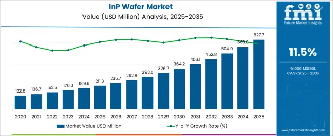
The InP Wafer Market is estimated to be valued at USD 211.3 million in 2025 and is projected to reach USD 627.7 million by 2035, registering a compound annual growth rate (CAGR) of 11.5% over the forecast period. The market will experience robust growth during the forecast period, with the first five years showing significant momentum. Between 2025 and 2026, the market will grow by USD 24.4 million, driven by increased demand for indium phosphide wafers in high-speed communication systems and optoelectronic devices. In 2026-2027, the market will expand by USD 26.2 million, as demand for advanced semiconductor technologies and optical devices increases, particularly in telecommunications and data centers.
From 2027 to 2028, the market will show a larger jump of USD 32.5 million, as the adoption of InP wafers accelerates in emerging applications like 5G technology and LiDAR systems. In 2028-2029, growth will continue at a strong pace, adding USD 33.7 million, as the need for high-performance, energy-efficient materials in electronics, automotive, and aerospace applications increases. By 2029-2030, the market will grow by USD 38.6 million, reaching USD 326.7 million. The increasing use of InP wafers in next-generation optical communications and quantum computing will contribute to sustained growth, with the market hitting USD 364.2 million by 2030. The first five years reflect strong adoption driven by both technological advancements and new applications in telecommunications and electronics.
Telecommunications infrastructure development presents intricate coordination challenges between equipment manufacturers operating under conflicting timeline pressures and performance specifications. Network operators demand optical transceivers capable of handling terabit data transmission rates while maintaining power efficiency targets that stress existing InP device capabilities. Engineering teams specify advanced InP-based photonic integrated circuits requiring precise wavelength control and minimal optical losses, yet procurement departments focus on cost competitiveness against alternative materials that may compromise long-term performance reliability. These tensions intensify during 5G network rollouts where deployment schedules conflict with device qualification protocols requiring months of testing under various operating conditions.
Fiber optic communications systems reveal fundamental tensions between performance optimization and cost management objectives. System integrators require InP laser diodes and photodetectors with specific wavelength characteristics and power output specifications while telecommunications service providers pursue capital expenditure reductions that pressure suppliers to minimize wafer costs. Quality assurance departments establish stringent reliability requirements based on decades of operation in harsh environments, creating procurement challenges where wafer selection decisions impact long-term maintenance costs and service availability metrics. Temperature cycling and humidity exposure testing becomes critical where laboratory conditions may not replicate actual deployment environments across diverse geographic regions.
| Metric | Value |
|---|---|
| InP Wafer Market Estimated Value in (2025 E) | USD 211.3 million |
| InP Wafer Market Forecast Value in (2035 F) | USD 627.7 million |
| Forecast CAGR (2025 to 2035) | 11.5% |
The InP wafer market is witnessing strong traction driven by rising adoption of high-frequency and optoelectronic components across telecom, datacenter, and sensing applications. Indium Phosphide has become an essential material for manufacturing photonic integrated circuits and high-electron-mobility transistors due to its superior electron velocity, direct bandgap, and ability to operate efficiently at high frequencies. The material’s importance has been underscored by growing investments in 5G backhaul, fiber-to-the-home (FTTH), and transceiver modules for cloud computing infrastructure.
Additionally, InP’s role in powering next-generation LiDAR, quantum photonics, and terahertz imaging has gained prominence in defense and autonomous systems. As global demand for low-latency and high-bandwidth communication expands, InP wafers are increasingly being integrated in telecom hardware, optical amplifiers, and photodetectors.
Moreover, advancements in epitaxial growth and defect control have enhanced wafer yields and scalability, enabling cost optimization in commercial production Strategic collaborations among fabless design houses, foundries, and substrate providers are expected to further strengthen the market outlook over the coming years.
The InP wafer market is segmented by diameter, product type, end-user industry, application, and geographic regions. By diameter, InP wafer market is divided into 100 mm (4") and Above, 76.2 mm (3"), and 50.8 mm (2"). In terms of product type, InP wafer market is classified into Semi-Insulating InP Wafer, N-Type InP Wafer, and P-Type InP Wafer. Based on end-user industry, InP wafer market is segmented into Telecommunications, Consumer electronics, Medical, and Others.
By application, InP wafer market is segmented into Optoelectronics, Photonic integrated circuits, RF/Microwave devices, Power electronics, Research & development, and Others. Regionally, the InP wafer industry is classified into North America, Latin America, Western Europe, Eastern Europe, Balkan & Baltic Countries, Russia & Belarus, Central Asia, East Asia, South Asia & Pacific, and the Middle East & Africa.
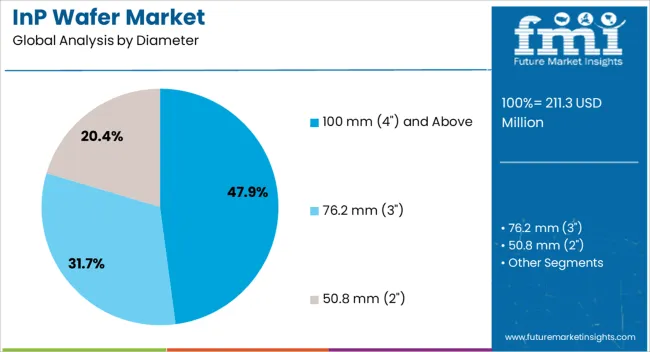
The 100 mm (4") and above diameter segment is projected to account for 47.9% of the total revenue share in the InP wafer market by 2025, reflecting its growing prominence in high-performance applications. This segment’s growth is being driven by increasing requirements for larger wafer formats that enable higher throughput and improved cost-per-chip economics in optical and RF semiconductor production.
Larger diameter wafers have allowed greater scalability in volume manufacturing, supporting automated processing and reducing material wastage. InP wafers of 100 mm and above are increasingly being adopted in the fabrication of laser diodes, photodetectors, and modulators where uniformity, thermal conductivity, and crystalline integrity are critical.
Advancements in wafer planarization and defect reduction techniques have enabled enhanced yields in these larger substrates. The rising integration of InP-based components in high-speed data transmission, especially in telecom infrastructure and high-speed computing interconnects, is reinforcing the demand for these larger diameter wafers across global manufacturing ecosystems.
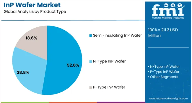
The semi-insulating InP wafer segment is expected to hold 52.6% of the revenue share in the InP wafer market by 2025, making it the leading product type. The dominance of this segment is attributed to its essential role in high-frequency electronics and optoelectronic devices, where low parasitic capacitance and high resistivity are required.
Semi-insulating substrates have enabled improved isolation in RF components, photonic integrated circuits, and avalanche photodiodes used in advanced telecommunication systems. These wafers offer superior thermal stability and electrical performance, supporting signal integrity in applications requiring high gain and low noise.
Their compatibility with advanced epitaxial layers and integration with compound semiconductor heterostructures has made them indispensable in high-reliability optoelectronic modules. Growing deployment of 5G base stations and satellite communication systems has elevated demand for semi-insulating InP wafers, which allow stable operation in harsh environments and across wide bandwidths, thereby reinforcing their leadership within the product category.
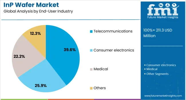
The telecommunications end-user segment is forecasted to account for 39.6% of the total revenue share in the InP wafer market by 2025, establishing it as the most dominant end-use industry. This leadership is being driven by the escalating need for high-speed, low-latency data transmission in fiber-optic networks, mobile backhaul, and optical interconnects.
Indium Phosphide-based devices have been widely adopted in telecom infrastructure for their efficiency in converting electrical signals into optical ones at very high speeds. The increasing global rollout of 5G networks, along with expanding bandwidth requirements from cloud services and video streaming, has further amplified the demand for InP wafers.
The ability of InP-based photonic devices to operate at higher frequencies with minimal signal degradation has positioned them as critical enablers in next-generation optical communication systems. Enhanced investment in data highways, submarine cable systems, and network densification is expected to maintain sustained demand from telecommunications OEMs and integrators, thereby reinforcing the segment’s leading position.
The InP wafer technology is experiencing steady growth, driven by increased demand in sectors like telecommunications, data centers, automotive, and consumer electronics. Technological advancements and the rise of 5G networks are further propelling growth, with InP wafers being essential for high-speed data transmission and advanced sensing capabilities. Although challenges such as high production costs and integration complexities persist, opportunities in emerging fields like quantum computing and LiDAR systems provide a promising outlook for the technology. The continued evolution of these technologies will contribute to the sustained innovation and expansion of InP wafer solutions in the coming years.
The demand for InP wafers is primarily driven by telecommunications and data centers, where the demand for high-speed data transmission, particularly for 5G networks, is accelerating. InP wafers play a critical role in manufacturing high-performance optoelectronic devices, including lasers and photodetectors. The automotive sector contributes significantly to this demand, especially with the rise of autonomous vehicles and advanced driver-assistance systems (ADAS), which require InP-based LiDAR sensors. InP’s unique electronic properties make it an ideal candidate for quantum computing, boosting research and development investments. The growing need for compact and efficient photonic components in consumer electronics also supports the adoption of InP wafers across industries.
InP wafer technology faces several challenges, particularly the high production costs associated with its complex manufacturing processes and the use of indium, a scarce and costly material. This makes InP wafers more expensive than other semiconductor materials, hindering their adoption in price-sensitive applications. Integration with existing technologies also poses difficulties, as InP-based components may have compatibility issues that require significant engineering efforts. Achieving high precision in wafer fabrication is essential to ensure device performance, but slight defects can lead to lower yields. Environmental concerns related to indium extraction and processing are also prompting the industry to adopt more sustainable practices, which adds another layer of complexity to production.
InP wafer technology offers substantial growth opportunities, particularly in emerging fields such as quantum computing, where its unique properties are being explored for next-generation computing systems. The ongoing demand for advanced communication technologies further boosts the application of InP wafers. Geographic expansion in regions like Asia-Pacific presents significant market potential, as semiconductor industries continue to grow in these areas. Moreover, innovations in wafer manufacturing processes and strategic partnerships between semiconductor manufacturers and research institutions will likely accelerate the development and adoption of InP-based technologies. These advancements are expected to lead to cost reductions and improved performance, expanding InP wafer applications across various industries.
Miniaturization is one of the key trends shaping the future of InP wafers. As electronic devices become smaller and more integrated, the need for compact and efficient InP-based components is increasing. The adoption of automation in wafer manufacturing is also on the rise, which is improving precision and scalability, allowing manufacturers to meet the growing demand for InP wafers. Additionally, there is a growing emphasis on sustainability within the semiconductor industry, driving the need for eco-friendly production practices, such as recycling and reducing the environmental impact of InP wafer fabrication. Customization of InP wafers to suit specific application requirements is also gaining momentum, driven by advancements in material science and fabrication techniques.
| Country | CAGR |
|---|---|
| China | 15.5% |
| India | 14.4% |
| Germany | 13.2% |
| France | 12.1% |
| UK | 10.9% |
| USA | 9.8% |
| Brazil | 8.6% |
The global InP wafer market is projected to grow at a CAGR of 11.5% from 2025 to 2035. Among the key markets, China leads with a growth rate of 15.5%, followed by India at 14.4%, and France at 12.1%. The United Kingdom and the United States record more moderate growth rates at 10.9% and 9.8%, respectively. This divergence highlights the accelerating adoption of InP wafers in emerging markets like China and India, driven by advancements in telecommunications, electronics, and photonics industries. In contrast, developed markets such as the USA and the UK continue to experience steady demand due to the establishment of advanced semiconductor manufacturing and electronic systems. The analysis spans over 40+ countries, with the leading markets shown below.
China is expected to lead the global InP wafer market, with a projected growth rate of 15.5% CAGR from 2025 to 2035. The country’s rapid expansion of its telecommunications and semiconductor industries is a significant factor driving this growth. China’s investments in advanced technologies, particularly in high-speed networks, optoelectronics, and optical communication systems, are creating high demand for InP wafers. The government’s push to develop cutting-edge electronic and photonic components is further accelerating the adoption of InP wafers, positioning China as a central player in the global market.
Demand for InP wafer in India is set to grow at a strong pace, with a projected CAGR of 14.4% from 2025 to 2035. The increasing demand for advanced electronic components in telecommunications, consumer electronics, and industrial applications is a primary growth driver. The rise of 5G technology, along with advancements in photonics and optoelectronics, is further accelerating the need for InP wafers in India. As the country continues to invest in its semiconductor manufacturing capabilities and infrastructure, the adoption of InP wafers in high-performance applications will continue to rise, reinforcing India’s position in the global market.
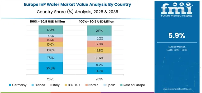
Sale of InP wafer in India is projected to grow at a steady pace, with a CAGR of 12.1% from 2025 to 2035. The country’s strong presence in the aerospace, telecommunications, and electronics industries continues to drive the demand for InP wafers. France’s commitment to expanding its semiconductor manufacturing capabilities and advancing optical communication technologies is increasing the adoption of InP wafers in various applications. The development of 5G infrastructure and optoelectronic systems further contributes to the market’s growth potential.
The United Kingdom’s InP wafer market is projected to grow at a CAGR of 10.9% from 2025 to 2035. The country’s strong presence in telecommunications and high-tech industries continues to drive the adoption of InP wafers in photonic and optoelectronic applications. The UK’s focus on developing 5G infrastructure and high-performance electronics is further fueling the demand for InP wafers. As the UK continues to expand its semiconductor and photonics sectors, InP wafers will play a crucial role in enhancing the performance and efficiency of next-generation communication and electronics systems.
The InP wafer market in the United States is projected to grow at a CAGR of 9.8% from 2025 to 2035. The demand for InP wafers in the USA is driven by advancements in the semiconductor and telecommunications industries, particularly in high-speed communication and optoelectronics applications. The rise of 5G networks and the continued development of photonic systems are further contributing to the market’s expansion. As the USA leads in technological innovation, the need for high-performance materials like InP wafers will continue to grow, supporting the growth of the global market.
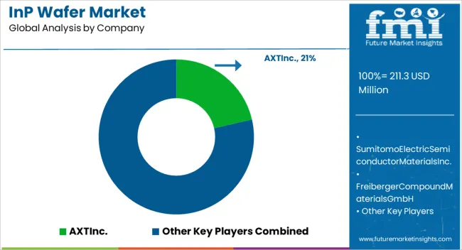
The Indium Phosphide (InP) Wafer Market is expanding rapidly, driven by the accelerating adoption of high-speed optoelectronic and communication technologies. InP wafers are essential substrates for fabricating photonic and electronic devices such as laser diodes, photodetectors, and high-frequency transistors. Their superior electron mobility, direct bandgap, and thermal stability make them indispensable for next-generation applications in 5G networks, data centers, optical fiber communication, and advanced sensing systems. The market’s growth is fueled by the global transition toward high-bandwidth connectivity and the increasing integration of photonics into consumer and industrial electronics.
Leading manufacturers such as AXT Inc., Sumitomo Electric Semiconductor Materials Inc., and Freiberger Compound Materials GmbH dominate global InP wafer production through advanced crystal growth technologies and vertically integrated supply chains. AXT Inc. specializes in vertical gradient freeze (VGF) InP wafers used in high-speed optical communication and LiDAR systems, while Sumitomo Electric focuses on ultra-high purity wafers with superior uniformity for photonic integrated circuits (PICs). Freiberger Compound Materials GmbH leads in semi-insulating and doped InP substrates catering to high-frequency and optoelectronic applications.
JX Nippon Mining & Metals Corporation and DOWA Electronics Materials Co. Ltd. are expanding capacity in Asia, supplying high-quality InP wafers to semiconductor foundries and photonics companies serving 5G and data center markets. Xiamen Powerway Advanced Material Co. Ltd. and Wafer Technology Ltd. provide cost-effective, custom-engineered InP substrates for research and industrial applications, supporting the growing global supply chain.
| Item | Value |
|---|---|
| Quantitative Units | USD 211.3 Million |
| Diameter | 100 mm (4") and Above, 76.2 mm (3"), and 50.8 mm (2") |
| Product Type | Semi-Insulating InP Wafer, N-Type InP Wafer, and P-Type InP Wafer |
| End-User Industry | Telecommunications, Consumer electronics, Medical, and Others |
| Application | Optoelectronics, Photonic integrated circuits, RF/ Microwave devices, Power electronics, Research & development, and Others |
| Regions Covered | North America, Europe, Asia-Pacific, Latin America, Middle East & Africa |
| Country Covered | United States, Canada, Germany, France, United Kingdom, China, Japan, India, Brazil, South Africa |
| Key Companies Profiled |
AXT Inc., Sumitomo Electric Semiconductor Materials Inc., Freiberger Compound Materials GmbH, JX Nippon Mining & Metals Corporation, Xiamen Powerway Advanced Material Co. Ltd., Wafer Technology Ltd., DOWA Electronics Materials Co. Ltd. |
| Additional Attributes | Dollar sales by product type (optical communication, semiconductor devices, photovoltaic applications) and end-use segments (telecommunications, electronics, aerospace). Demand dynamics are driven by the rising need for high-speed data transmission, increased demand for 5G technologies, and advancements in optoelectronic devices. Regional trends indicate strong growth in Asia-Pacific, particularly Japan and China, due to increased investments in 5G and fiber optic communication systems. North America and Europe are also experiencing growth, supported by advancements in semiconductor technologies and the demand for high-performance InP wafers in advanced electronics. |
How big is the InP wafer market in 2025?
The global InP wafer market is estimated to be valued at USD 211.3 million in 2025.
What will be the size of InP wafer market in 2035?
The market size for the InP wafer market is projected to reach USD 627.7 million by 2035.
How much will be the InP wafer market growth between 2025 and 2035?
The InP wafer market is expected to grow at a 11.5% CAGR between 2025 and 2035.
What are the key product types in the InP wafer market?
The key product types in InP wafer market are 100 mm (4") and above, 76.2 mm (3") and 50.8 mm (2").
Which product type segment to contribute significant share in the InP wafer market in 2025?
In terms of product type, semi-insulating InP wafer segment to command 52.6% share in the InP wafer market in 2025.
Full Research Suite comprises of:
Market outlook & trends analysis
Interviews & case studies
Strategic recommendations
Vendor profiles & capabilities analysis
5-year forecasts
8 regions and 60+ country-level data splits
Market segment data splits
12 months of continuous data updates
DELIVERED AS:
PDF EXCEL ONLINE

Thank you!
You will receive an email from our Business Development Manager. Please be sure to check your SPAM/JUNK folder too.