- Market Size (2026)
- USD 1.7 Bn
- Forecast (2036)
- USD 6.1 Bn
- CAGR (2026 to 2036)
- 13.6%
How big is the Chiplet Inspection Metrology Market in 2026?
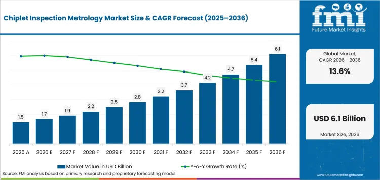
USD 1.7 billion in 2026 and USD 6.1 billion by 2036 at a 13.6% CAGR.
Demand for chiplet inspection metrology is projected to expand at 13.6% CAGR between 2026 and 2036, increasing valuation from USD 1.7 billion in 2026 to USD 6.1 billion by 2036. More inspection steps become necessary as semiconductor manufacturing equipment supports packages containing several separately fabricated dies.
Advanced packaging concentrates more functional value behind each inspection decision and increases the financial effect of an escaped defect. SEMI counted 750 assembly and test facilities in July 2025, representing 70 additional sites from its previous edition. Production teams therefore combine semiconductor metrology and inspection coverage with targeted electron-beam or X-ray review across expanding packaging networks.
Key Takeaways of Chiplet Inspection Metrology Market
- Inspection demand rises as foundries protect accumulated die value across pre-bond and post-bond control points.
- Optical inspection is projected to represent 37.0% in 2026 due to rapid wafer and package-surface screening.
- Advanced semiconductor packaging is estimated to capture 34.0% in 2026 owing to stacked structures that add inspection interfaces.
- Semiconductor foundries are forecast to account for 39.0% in 2026 driven by high-volume process-control responsibilities.
- Higher resolution or penetration depth reduces throughput and requires risk-based modality combinations across production control points.
- KLA Corporation, Onto Innovation Inc., Applied Materials, Hitachi High-Tech, Lasertec, Nova, Camtek and ZEISS provide verified inspection or metrology workflows for advanced semiconductor production.
Analyst Perspective
“Inspection priorities change materially as chiplet packages accumulate bonded die value across successive assembly stages. Process teams protect yield by matching optical screening, dimensional metrology and internal imaging to the defect mechanism exposed at each control point.”
- Nikhil Kaitwade, Principal Analyst, Future Market Insights
How is the Chiplet Inspection Metrology Market segmented?
The chiplet inspection metrology industry is segmented by inspection technology, application, end user, distribution channel, metrology type and region.
Inspection technology covers optical, electron-beam, X-ray and hybrid systems across advanced packaging, chiplet manufacturing, wafer inspection and package failure analysis. End users include foundries, integrated device manufacturers, OSAT companies and research institutes, while channels cover direct sales, distributors, integrators and online sales. Metrology types include dimensional, defect, material and overlay or alignment measurement across wafer and package control stages.
How does optical inspection shape demand within the inspection technology category?
Broad-area wafer inspection systems locate suspect coordinates before slower methods consume cycle time across production lots. Their screening role supports rapid recipe feedback across patterned wafers, singulated dies and assembled package surfaces during successive product generations.
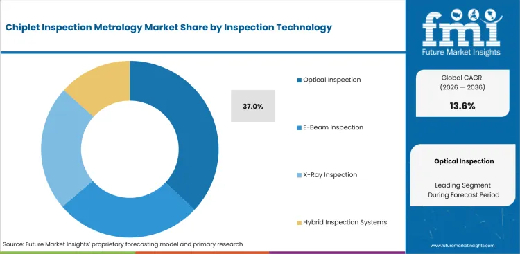
- Optical inspection is set to lead the inspection technology category with 37.0% share in 2026 due to rapid whole-surface screening across production lots.
- Two-dimensional imaging classifies surface defects quickly across package surfaces, while three-dimensional methods measure bump height and topography. Defect inspection equipment then directs detailed review toward locations carrying greater package-yield risk without delaying routine lot release across high-volume manufacturing programs.
What makes advanced semiconductor packaging central to the application category?
Advanced packaging combines logic dies with memory stacks and interposers across 3D TSV packages in production. Each interface introduces alignment, bonding and hidden-structure conditions that require inspection at several assembly stages.
- By application, advanced semiconductor packaging is estimated to hold 34.0% in 2026 owing to stacked designs that multiply surfaces and buried connections.
- Qualification teams compare pre-bond cleanliness with post-bond alignment and final package integrity across assembly stages. Onto Innovation documented Dragonfly G5 qualification for two 2.5D packaging applications in April 2026 at customer sites. The result connects adaptable optics with chiplet interconnect testing across changing package layouts and worldwide customer production sites.
How do semiconductor foundries evaluate inspection requirements within the end-user category?
Foundries control wafer fabrication and qualify inspection recipes as dies approach higher-value package assembly stages. Their engineers connect semiconductor inspection systems with design rules and yield-learning records across logic and memory generations during customer production transfers.
- The semiconductor foundries segment is likely to capture 39.0% share in 2026 attributable to high-volume operations that require early defect excursion control.
- Foundries transfer approved recipes to assembly and testing services partners through controlled production data formats. Recipe ownership lets process teams compare defect patterns with process changes without repeating full qualification at every customer site during scheduled product and manufacturing-site transitions.
What role does dimensional metrology play within the metrology type category?
Dimensional metrology checks feature size and relative position ahead of wafer-to-wafer or die-to-wafer assembly across semiconductor bonding equipment. NIST reported in January 2026 that hybrid-bonding-ready copper pads require nanoscale mechanical characterization for predictive manufacturing control.
- By metrology type, dimensional metrology is forecast to represent 36.0% in 2026 driven by critical-dimension and package-alignment requirements.
- Process engineers compare bump height and overlay records across several package integration stages during production. Corrective action limits electrical opens or shorts before dimensional drift reaches final package testing during volume production. Those records also support reliable recipe transfer across tools and customer sites during package ramp-up and recurring production reviews.
What are the drivers, restraints and opportunities in the Chiplet Inspection Metrology Market?
Rising package value increases inspection intensity as modality tradeoffs limit coverage and coordinated workflows target high-risk coordinates.
- Driver: Each added die increases package value exposed to defects that escape earlier assembly control points.
- Restraint: No inspection modality combines maximum throughput with resolution and internal visibility across every package structure.
- Opportunity: Connected inspection records route suspect coordinates toward detailed review without slowing complete production lots.
Multi-die assembly concentrates recoverable value behind inspection decisions made upstream of final electrical testing stages. Onto Innovation reported more than twenty Dragonfly shipments for advanced AI packaging in August 2025. Wider production placement increases recipe-transfer requirements across packaging layers and customer manufacturing sites during volume ramps.
Optical platforms screen broad surfaces rapidly but lose sensitivity for buried structures and extremely small defects. Electron-beam or X-ray review improves detail at lower throughput, so process teams assign each method to the failure mode that justifies its cycle time.
Connected inspection records route suspect coordinates from broad screening toward detailed review across production control stages. Shared data links defects with specific process steps and helps engineers revise control limits before recurring failures spread across production lots.
Which country CAGRs are profiled in the Chiplet Inspection Metrology Market?
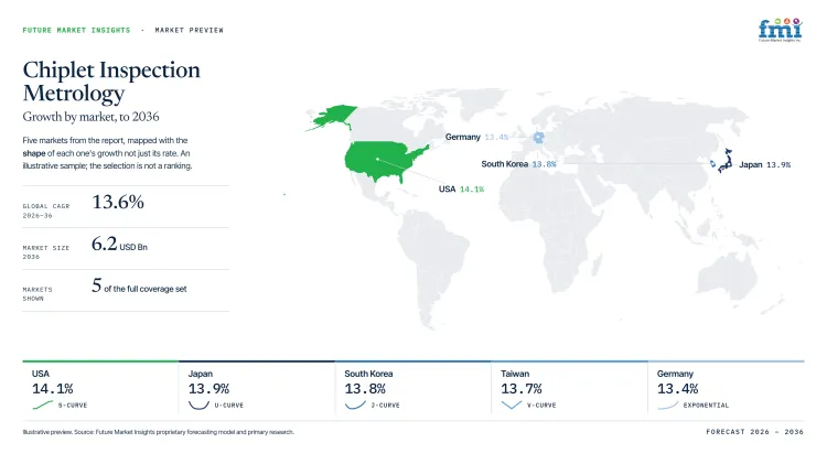
| Country | CAGR |
|---|---|
| United States | 14.1% |
| Japan | 13.9% |
| Taiwan | 13.7% |
| Germany | 13.4% |
| Singapore | 13.2% |
How do country-level CAGRs compare in the Chiplet Inspection Metrology Market?
The displayed country CAGRs span 0.9 percentage point across established semiconductor manufacturing and research systems. Their narrow spacing describes forecast pace without proving present market size or installed inspection capacity.
- United States growth reflects public packaging programs connecting domestic tool evaluation with manufacturing transfer across regional production clusters.
- Japan's 0.2-point difference reflects established metrology expertise and qualification work across advanced packaging programs and customer facilities.
- Taiwan records a further 0.2-point interval as dense foundry capacity shortens feedback between recipe trials and production lines.
- Germany's 0.3-point separation reflects pilot-line access that connects chiplet research with industrial measurement development programs.
- Singapore's 0.2-point interval reflects packaging activity that requires multinational approval and responsive regional application support.
Comparable CAGRs can produce different entry conditions across semiconductor production networks and equipment service models.
The full report covers country-level growth across every standard FMI region and its defined national markets.
Country-wise Analysis
- United States foundries and packaging pilot lines qualify inspection platforms through domestic research programs that connect laboratory measurements with production transfer across regional manufacturing clusters and customer qualification sites during scheduled production programs. The United States is estimated to post 14.1% CAGR over the forecast period, supported by NIST awards totaling USD 1.4 billion for advanced packaging commercialization across domestic consortium projects in January 2025. Public funding expands early tool evaluation, although inspection-equipment manufacturers must demonstrate production throughput and maintain application support across distant facilities before engineering trials convert into repeat orders during high-volume customer ramps and qualification cycles.
- Japanese semiconductor manufacturers evaluate inspection platforms through precise process-control routines and localized application teams serving concentrated logic, memory and packaging clusters supported by domestic equipment engineering and research networks throughout Japan's principal industrial regions. Adoption of chiplet inspection metrology in Japan is estimated to expand at 13.9% CAGR through 2036, reinforced by domestic metrology expertise and coordinated qualification across customer facilities and specialized production programs. METI included heterogeneous integration and chiplets in its May 2025 partnership agenda, yet local qualification depends on translated documentation and stable recipe performance before engineering trials convert into production orders at domestic manufacturing sites.
- Taiwanese foundries and packaging lines evaluate inspection recipes near high-volume process owners through connected science parks and application teams serving advanced logic and memory programs during accelerated qualification cycles across several domestic production regions. Taiwan's chiplet inspection metrology outlook is anticipated to advance at 13.7% CAGR over the assessment period, driven by TSMC's April 2026 development across CoWoS and InFO with SoIC production lines at major sites. Concentrated production shortens qualification cycles, but regional application teams must preserve recipe stability across rapid package transitions and maintain responsive service during scheduled factory ramps across multiple customer sites and product generations.
- German research institutes and equipment engineers use specialized pilot lines to connect chiplet integration experiments with traceable measurement routines and industrial transfer requirements across European advanced packaging programs and regional industrial manufacturing networks. Chiplet inspection metrology sales in Germany are forecast to expand at 13.4% CAGR by 2036, supported by APECS wafer-level chiplet work reported by Fraunhofer IPMS across pilot and industrial projects in May 2026. Pilot-line access supports measurement development across APECS projects, whereas commercial orders depend on repeatable production controls and trained application engineers supported by dependable regional service routes and local technical training for industrial customers.
- Singapore combines multinational assembly operations with research institutes and regional logistics that support memory packaging qualification across outsourced production networks and specialized semiconductor service hubs serving Asian manufacturing programs and customer production transfers. The Singapore chiplet inspection metrology sector is projected to record 13.2% CAGR during the assessment period, influenced by Micron's HBM packaging facility announced by the Economic Development Board for operations in January 2025. Corporate approval chains remain a material friction despite new capacity, requiring platform providers to prove recipe transfer between Singapore facilities and overseas production sites during coordinated volume ramps and major customer schedules worldwide.
Who are the notable companies in the Chiplet Inspection Metrology Market?
KLA Corporation, Onto Innovation Inc., Applied Materials, Inc., Hitachi High-Tech Corporation, Lasertec Corporation, Nova Ltd., Camtek Ltd. and ZEISS Group are the notable companies serving this market.
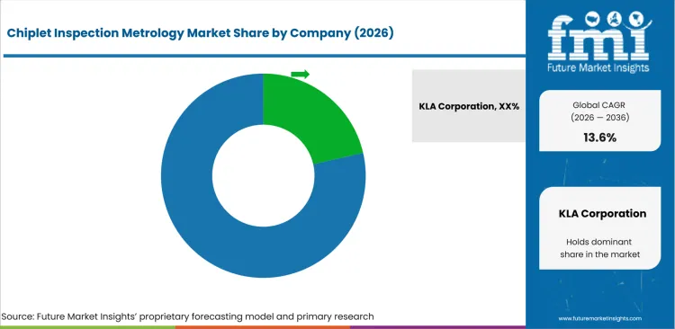
Competition is moderately concentrated among process-control specialists and imaging companies that address different defect depths across advanced package structures. Entry requires semiconductor-qualified hardware with repeatable recipes and responsive local application support during customer qualification. Production sites therefore qualify complementary systems because broad optical screening, nanoscale dimensional control and internal package imaging operate at different throughput levels.
- KLA Corporation and Onto Innovation combine surface inspection with dimensional metrology, while Camtek concentrates on high-throughput advanced packaging control.
- Applied Materials links electron-beam control with stacked-package workflows, while Hitachi High-Tech combines wafer inspection with semiconductor analysis equipment.
- Nova measures warped package geometry, while Lasertec and ZEISS provide infrared or X-ray access to internal structures.
Competitive Benchmarking: Chiplet Inspection Metrology Market
| Company | Surface Inspection and Dimensional Metrology | Subsurface and 3D Analysis | Chiplet and Advanced Packaging Coverage | Geographic Reach |
|---|---|---|---|---|
| KLA Corporation | High | Medium | High | Global |
| Onto Innovation Inc. | High | High | High | Global |
| Applied Materials, Inc. | High | Low | High | Global |
| Hitachi High-Tech Corporation | High | Medium | Medium | Global |
| Lasertec Corporation | Medium | High | High | Global |
| Nova Ltd. | High | Medium | High | Global |
| Camtek Ltd. | High | Low | High | Global |
| ZEISS Group | Medium | High | High | Global |
Key Developments in the Chiplet Inspection Metrology Market
- In August 2025, Nova released the Nova WMC, a modular optical metrology platform purpose-built for 2.5D/3D advanced packaging, already adopted by a leading HBM memory manufacturer.
- In June 2026, Applied Materials introduced eBeam metrology and defect-review systems that extend wafer-fab-grade process control into advanced packaging.
- In March 2026, Camtek received a USD 31 million multi-system order from a leading OSAT for CoWoS-like advanced packaging, bringing total Q1 2026 OSAT orders above USD 90 million.
Key Players in the Chiplet Inspection Metrology Market
Integrated Process-Control Platforms
- KLA Corporation
- Applied Materials, Inc.
- Hitachi High-Tech Corporation
Advanced Packaging Inspection and Metrology Specialists
- Onto Innovation Inc.
- Nova Ltd.
- Camtek Ltd.
Internal Imaging and Failure-Analysis Platforms
- Lasertec Corporation
- ZEISS Group
Chiplet Inspection Metrology Market - Report Scope
| Coverage field | Report scope |
|---|---|
| Market breakdown | By inspection technology, application, end user, distribution channel, metrology type and region. |
| Quantitative Units | Revenue in USD billion and CAGR in %. |
| Market Definition | Equipment used to inspect or measure chiplet structures across wafer, die, package and failure-analysis stages. |
| Regions Covered | North America, Latin America, Europe, East Asia, South Asia and Pacific, and Middle East and Africa. |
| Countries Covered | United States, Japan, Taiwan, Germany, Singapore, and 20+ countries in the full report. |
| Key Companies Profiled | KLA, Onto Innovation, Applied Materials, Hitachi High-Tech, Lasertec, Nova, Camtek and ZEISS. |
| Forecast Period | 2026 to 2036. |
| Approach | Primary and secondary research with market triangulation. |
Chiplet Inspection Metrology Market - Research Methodology
| Method | Approach |
|---|---|
| Primary Research | FMI analysts gathered input from manufacturers, service providers, technology developers, distributors, end users, procurement teams, and subject-matter experts. Interviews examined purchasing decisions, product or service evaluation, adoption barriers, approval requirements, pricing considerations, and expectations for technical or commercial support. Respondents were also asked what evidence is required before a trial, pilot, or initial order develops into regular purchasing. |
| Desk Research | Desk research covered government statistics, regulatory publications, trade data, industry associations, technical literature, standards, company filings, product information, and official corporate announcements. Sources were reviewed for relevance, publication date, geographic coverage, and consistency with the defined market scope. Claims relating to performance, applications, approvals, capacity, investment, and commercial activity were retained only when supported by credible public evidence. |
| Market Sizing and Forecasting | The market model combined the baseline value with historical performance, segment structure, pricing and volume indicators, adoption levels, company participation, and country-level demand conditions. Forecast assumptions considered economic activity, investment trends, regulatory developments, technology adoption, purchasing cycles, supply availability, and barriers to wider market use. Segment and regional estimates were reconciled before the final market total was calculated. |
| Data Validation | Estimates were checked against multiple independent indicators, including public data, company activity, trade patterns, industry developments, and findings from primary interviews. Validation also tested whether products, services, applications, and company revenues fell within the defined market boundaries. Adjacent categories, unsupported claims, overlapping revenues, and activities without direct market relevance were excluded to reduce double counting and maintain consistency across segments and countries. |
Chiplet Inspection Metrology Market by Segments
Chiplet Inspection Metrology Market segmented by Inspection Technology:
- Optical Inspection
- 2D Optical Inspection
- 3D Optical Inspection
- E-Beam Inspection
- CD-SEM Inspection
- High-Resolution Defect Inspection
- X-Ray Inspection
- 2D X-Ray Inspection
- 3D X-Ray Computed Tomography
- Hybrid Inspection Systems
- Optical-E-Beam Systems
- AI-Assisted Inspection Systems
Chiplet Inspection Metrology Market segmented by Application:
- Advanced Semiconductor Packaging
- 2.5D Packaging
- 3D Packaging
- Chiplet Manufacturing
- Heterogeneous Integration
- Multi-Die Integration
- Wafer Inspection
- Front-End Wafer Inspection
- Back-End Wafer Inspection
- Package Failure Analysis
- Defect Characterization
- Reliability Testing
Chiplet Inspection Metrology Market segmented by End User:
- Semiconductor Foundries
- Logic Foundries
- Memory Foundries
- Integrated Device Manufacturers (IDMs)
- Logic Device Manufacturers
- Analog Device Manufacturers
- OSAT Companies
- Assembly Service Providers
- Test Service Providers
- Research Institutes
- National Laboratories
- University Research Centers
Chiplet Inspection Metrology Market segmented by Distribution Channel:
- Direct Sales
- OEM Supply Agreements
- Key Account Sales
- Authorized Distributors
- Regional Distributors
- Global Equipment Dealers
- System Integrators
- Semiconductor Integration Partners
- Automation Solution Providers
- Online Sales
- Manufacturer Websites
- B2B E-Commerce Platforms
Chiplet Inspection Metrology Market segmented by Metrology Type:
- Dimensional Metrology
- Critical Dimension Measurement
- Overlay Measurement
- Defect Metrology
- Surface Defect Inspection
- Particle Detection
- Material Metrology
- Film Thickness Measurement
- Material Composition Analysis
- Overlay & Alignment Metrology
- Wafer Alignment
- Package Alignment
Chiplet Inspection Metrology Market by Region:
- North America
- United States
- Canada
- Mexico
- Latin America
- Brazil
- Chile
- Rest of Latin America
- Western Europe
- Germany
- United Kingdom
- Italy
- Spain
- France
- Nordics
- Benelux
- Rest of Western Europe
- Eastern Europe
- Russia
- Poland
- Hungary
- Balkan and Baltic States
- Rest of Eastern Europe
- East Asia
- China
- Japan
- South Korea
- South Asia and Pacific
- India
- ASEAN
- Australia and New Zealand
- Rest of South Asia and Pacific
- Middle East and Africa
- Kingdom of Saudi Arabia
- Other GCC Countries
- Türkiye
- South Africa
- Other African Union Countries
- Rest of Middle East and Africa
Research Sources and Bibliography
- SEMI. (2025, July 1). SEMI and TechSearch International Release 2025 Edition of Worldwide Semiconductor Assembly & Test Facility Database.
- Onto Innovation Inc. (2026, April 16). Onto Innovation’s Dragonfly G5 System Qualified for Applications in 2.5D AI Packaging.
- National Institute of Standards and Technology. (2026, January 29). Nanoscale Mechanical Characterization for Hybrid-Bonding-Ready Structures in Advanced Packaging.
- Onto Innovation Inc. (2025, August 7). Onto Innovation Reports 2025 Second Quarter Results.
- National Institute of Standards and Technology. (2025, January 16). USA Department of Commerce Announces $1.4 Billion in Final Awards to Support the Next Generation of USA Semiconductor Advanced Packaging.
- Ministry of Economy, Trade and Industry. (2025, May 13). Third Ministerial Meeting of the Japan-EU Digital Partnership Council Held.
- Taiwan Semiconductor Manufacturing Company Limited. (2026, April 16). TSMC 2025 Annual Report.
- Fraunhofer Institute for Photonic Microsystems. (2026, May 19). The Future of Chip Integration: Fraunhofer IPMS Develops High-Density Chiplet Systems at the Wafer Level.
- Singapore Economic Development Board. (2025, January 8). Micron Breaks Ground on High-Bandwidth-Memory Advanced Packaging Facility in Singapore.
- KLA Corporation. (2025, August 8). Annual Report for the Fiscal Year Ended June 30, 2025.
- Applied Materials, Inc. (2026, June 25). Applied Materials Introduces New Systems to Accelerate DRAM and Advanced Packaging for AI Chips.
- Hitachi High-Tech Corporation. (2025, October 31). Hitachi High-Tech Announces the SU9600: Next-Generation Ultrahigh-Resolution Scanning Electron Microscope with High Throughput.
- Lasertec Corporation. (2025, January 20). Lasertec Releases Infrared Confocal Microscope “OPTELICS IR”.
- Nova Ltd. (2026, July 2). Nova WMC Expanding Adoption Across the Most Advanced Packaging Processes.
- Camtek Ltd. (2026, June 2). Camtek Receives Over $105 Million Multi-System Orders from a Tier-1 OSAT and a Leading HBM Manufacturer.
- ZEISS Group. (2026, July 10). ZEISS Opens Semiconductor Innovation Center in Korea to Deepen Customer Collaboration.
- Onto Innovation Inc. (2026, March 16). Onto Innovation Launches Dragonfly G5 Inspection System.
- Nova Ltd. (2025, August 26). Nova Announces the Release of Nova WMC: A Next-Generation Modular Optical Metrology Platform for Advanced Packaging.
- Camtek Ltd. (2026, March 30). Camtek Receives $31 Million Multi-System Order from a Leading OSAT.
This bibliography is provided for reader reference and is not exhaustive. The full report contains the complete reference list and detailed citations.
This Report Answers
- How large is the global Chiplet Inspection Metrology market in 2026, and what value is forecast for 2036?
- Which industry and manufacturing conditions are supporting inspection and metrology spending across multi-die and chiplet-based packages?
- Which inspection technology segment holds the largest share of the market in 2026?
- How do advanced packaging architectures change inspection and metrology requirements across wafer, assembly, and packaging stages?
- Why do foundries account for a significant share of demand in the Chiplet Inspection Metrology market?
- How do market growth rates and adoption trends differ across the countries profiled in the report?
- Which leading companies provide inspection, metrology, internal imaging, and defect-analysis solutions for chiplet manufacturing?
- What technical limitations related to throughput, resolution, and penetration depth affect inspection and metrology performance?
Frequently Asked Questions
How big is the Chiplet Inspection Metrology Market in 2026?
In 2026, the chiplet inspection metrology market is valued at USD 1.7 billion across wafer and package control workflows. Higher inspection intensity supports the projected increase to USD 6.1 billion by 2036 as manufacturers protect accumulated value across multi-die assemblies.
What is the CAGR of the Chiplet Inspection Metrology Market from 2026 to 2036?
The chiplet inspection metrology market is projected to expand at 13.6% CAGR from 2026 to 2036 across semiconductor production. Forecast performance depends on practical throughput and reliable recipe transfer as foundries or packaging sites extend inspection coverage across increasingly complex package structures.
Which inspection technology is projected to account for 37.0% of the Chiplet Inspection Metrology Market?
Optical inspection is projected to account for 37.0% of the chiplet inspection metrology market by inspection technology in 2026. Broad surface coverage supports early screening as higher-resolution methods examine buried structures or locations carrying greater yield risk during package assembly.
How much will the Chiplet Inspection Metrology Market add between 2026 and 2036?
USD 4.4 billion is expected to be added to the chiplet inspection metrology market between 2026 and 2036. Added value depends on controlling defect escapes as stacked dies and fine interconnects increase the financial consequence of discovering failures late in assembly.
Which companies are active in the Chiplet Inspection Metrology Market?
Key providers active in the chiplet inspection metrology market across surface inspection, dimensional control and internal imaging include KLA Corporation, Onto Innovation, Applied Materials, Hitachi High-Tech, Lasertec, Nova, Camtek and ZEISS.
Preview the report firsthand - request a free sample
Get SampleGet the brochure for pricing and purchase details.
Get PDFTable of Content
- Key Takeaways
- Market Size and CAGR
- Top Growth Driver
- Fastest Growing Segment
- Leading Region
- Key Companies
- Emerging Opportunities
- Executive Summary
- Global Market Outlook
- Demand-side Trends
- Supply-side Trends
- Technology Roadmap Analysis
- Analysis and Recommendations
- Analyst Perspective (What is happening? Why now? What should investors know?)
- Key Questions Answered
- How large is the market?
- What is the CAGR?
- What are key trends?
- Which region dominates?
- Who are the leaders?
- Market Overview
- Market Coverage / Taxonomy
- Market Definition / Scope / Limitations
- Research Methodology
- Chapter Orientation
- Analytical Lens and Working Hypotheses
- Market Structure, Signals, and Trend Drivers
- Benchmarking and Cross-market Comparability
- Market Sizing, Forecasting, and Opportunity Mapping
- Research Design and Evidence Framework
- Desk Research Programme (Secondary Evidence)
- Expert Input and Fieldwork (Primary Evidence)
- Tooling, Models, and Reference Databases
- Data Engineering and Model Build
- Quality Assurance and Audit Trail
- Market Background
- Market Dynamics (Drivers, Restraints, Opportunity, Trends)
- Scenario Forecast (Optimistic, Likely, Conservative)
- Impact Analysis
- AI Impact
- Sustainability Impact
- Regulatory Impact
- Technology Impact
- Consumer / Buyer Analysis
- Purchase Drivers
- Adoption Barriers
- Buyer Journey
- Opportunity Map Analysis
- Product Life Cycle Analysis
- Supply Chain Analysis
- Investment Feasibility Matrix
- Value Chain Analysis
- PESTLE and Porter's Analysis
- Regulatory Landscape
- Regional Parent Market Outlook
- Production and Consumption Statistics
- Import and Export Statistics
- Global Market Analysis and Forecast, 2021 to 2036
- Historical Market Size Value (USD Billion) Analysis, 2021 to 2025
- Current and Future Market Size Value (USD Billion) Projections, 2026 to 2036
- Y-o-Y Growth Trend Analysis
- Absolute $ Opportunity Analysis
- Global Market Pricing Analysis, 2021 to 2036
- Global Market Analysis and Forecast, By Inspection Technology, 2021 to 2036
- Introduction / Key Findings
- Historical Market Size Value (USD Billion) Analysis By Inspection Technology, 2021 to 2025
- Current and Future Market Size Value (USD Billion) Analysis and Forecast By Inspection Technology, 2026 to 2036
- Optical Inspection
- 2D Optical Inspection
- 3D Optical Inspection
- E-Beam Inspection
- CD-SEM Inspection
- High-Resolution Defect Inspection
- X-Ray Inspection
- 2D X-Ray Inspection
- 3D X-Ray Computed Tomography
- Hybrid Inspection Systems
- Optical-E-Beam Systems
- AI-Assisted Inspection Systems
- Optical Inspection
- Y-o-Y Growth Trend Analysis By Inspection Technology, 2021 to 2025
- Absolute $ Opportunity Analysis By Inspection Technology, 2026 to 2036
- Global Market Analysis and Forecast, By Application, 2021 to 2036
- Introduction / Key Findings
- Historical Market Size Value (USD Billion) Analysis By Application, 2021 to 2025
- Current and Future Market Size Value (USD Billion) Analysis and Forecast By Application, 2026 to 2036
- Advanced Semiconductor Packaging
- 2.5D Packaging
- 3D Packaging
- Chiplet Manufacturing
- Heterogeneous Integration
- Multi-Die Integration
- Wafer Inspection
- Front-End Wafer Inspection
- Back-End Wafer Inspection
- Package Failure Analysis
- Defect Characterization
- Reliability Testing
- Advanced Semiconductor Packaging
- Y-o-Y Growth Trend Analysis By Application, 2021 to 2025
- Absolute $ Opportunity Analysis By Application, 2026 to 2036
- Global Market Analysis and Forecast, By End User, 2021 to 2036
- Introduction / Key Findings
- Historical Market Size Value (USD Billion) Analysis By End User, 2021 to 2025
- Current and Future Market Size Value (USD Billion) Analysis and Forecast By End User, 2026 to 2036
- Semiconductor Foundries
- Logic Foundries
- Memory Foundries
- Integrated Device Manufacturers (IDMs)
- Logic Device Manufacturers
- Analog Device Manufacturers
- OSAT Companies
- Assembly Service Providers
- Test Service Providers
- Research Institutes
- National Laboratories
- University Research Centers
- Semiconductor Foundries
- Y-o-Y Growth Trend Analysis By End User, 2021 to 2025
- Absolute $ Opportunity Analysis By End User, 2026 to 2036
- Global Market Analysis and Forecast, By Distribution Channel, 2021 to 2036
- Introduction / Key Findings
- Historical Market Size Value (USD Billion) Analysis By Distribution Channel, 2021 to 2025
- Current and Future Market Size Value (USD Billion) Analysis and Forecast By Distribution Channel, 2026 to 2036
- Direct Sales
- OEM Supply Agreements
- Key Account Sales
- Authorized Distributors
- Regional Distributors
- Global Equipment Dealers
- System Integrators
- Semiconductor Integration Partners
- Automation Solution Providers
- Online Sales
- Manufacturer Websites
- B2B E-Commerce Platforms
- Direct Sales
- Y-o-Y Growth Trend Analysis By Distribution Channel, 2021 to 2025
- Absolute $ Opportunity Analysis By Distribution Channel, 2026 to 2036
- Global Market Analysis and Forecast, By Metrology Type, 2021 to 2036
- Introduction / Key Findings
- Historical Market Size Value (USD Billion) Analysis By Metrology Type, 2021 to 2025
- Current and Future Market Size Value (USD Billion) Analysis and Forecast By Metrology Type, 2026 to 2036
- Dimensional Metrology
- Critical Dimension Measurement
- Overlay Measurement
- Defect Metrology
- Surface Defect Inspection
- Particle Detection
- Material Metrology
- Film Thickness Measurement
- Material Composition Analysis
- Overlay & Alignment Metrology
- Wafer Alignment
- Package Alignment
- Dimensional Metrology
- Y-o-Y Growth Trend Analysis By Metrology Type, 2021 to 2025
- Absolute $ Opportunity Analysis By Metrology Type, 2026 to 2036
- Global Market Analysis and Forecast, By Region, 2021 to 2036
- Introduction
- Historical Market Size Value (USD Billion) Analysis By Region, 2021 to 2025
- Current Market Size Value (USD Billion) Analysis and Forecast By Region, 2026 to 2036
- North America
- Latin America
- Western Europe
- Eastern Europe
- East Asia
- South Asia and Pacific
- Middle East & Africa
- Market Attractiveness Analysis By Region
- North America Market Analysis and Forecast, By Country, 2021 to 2036
- Historical Market Size Value (USD Billion) Trend Analysis By Market Taxonomy, 2021 to 2025
- Market Size Value (USD Billion) Forecast By Market Taxonomy, 2026 to 2036
- By Country
- USA
- Canada
- By Inspection Technology
- By Application
- By End User
- By Distribution Channel
- By Metrology Type
- By Country
- Market Attractiveness Analysis
- By Country
- By Inspection Technology
- By Application
- By End User
- By Distribution Channel
- By Metrology Type
- Key Takeaways
- Latin America Market Analysis and Forecast, By Country
- Historical Market Size Value (USD Billion) Trend Analysis By Market Taxonomy, 2021 to 2025
- Market Size Value (USD Billion) Forecast By Market Taxonomy, 2026 to 2036
- By Country
- Brazil
- Mexico
- Chile
- Rest of Latin America
- By Inspection Technology
- By Application
- By End User
- By Distribution Channel
- By Metrology Type
- By Country
- Market Attractiveness Analysis
- By Country
- By Inspection Technology
- By Application
- By End User
- By Distribution Channel
- By Metrology Type
- Key Takeaways
- Western Europe Market Analysis and Forecast, By Country
- Historical Market Size Value (USD Billion) Trend Analysis By Market Taxonomy, 2021 to 2025
- Market Size Value (USD Billion) Forecast By Market Taxonomy, 2026 to 2036
- By Country
- Germany
- UK
- Italy
- Spain
- France
- Nordic
- BENELUX
- Rest of Western Europe
- By Inspection Technology
- By Application
- By End User
- By Distribution Channel
- By Metrology Type
- By Country
- Market Attractiveness Analysis
- By Country
- By Inspection Technology
- By Application
- By End User
- By Distribution Channel
- By Metrology Type
- Key Takeaways
- Eastern Europe Market Analysis and Forecast, By Country
- Historical Market Size Value (USD Billion) Trend Analysis By Market Taxonomy, 2021 to 2025
- Market Size Value (USD Billion) Forecast By Market Taxonomy, 2026 to 2036
- By Country
- Russia
- Poland
- Hungary
- Balkan & Baltic
- Rest of Eastern Europe
- By Inspection Technology
- By Application
- By End User
- By Distribution Channel
- By Metrology Type
- By Country
- Market Attractiveness Analysis
- By Country
- By Inspection Technology
- By Application
- By End User
- By Distribution Channel
- By Metrology Type
- Key Takeaways
- East Asia Market Analysis and Forecast, By Country
- Historical Market Size Value (USD Billion) Trend Analysis By Market Taxonomy, 2021 to 2025
- Market Size Value (USD Billion) Forecast By Market Taxonomy, 2026 to 2036
- By Country
- China
- Japan
- South Korea
- By Inspection Technology
- By Application
- By End User
- By Distribution Channel
- By Metrology Type
- By Country
- Market Attractiveness Analysis
- By Country
- By Inspection Technology
- By Application
- By End User
- By Distribution Channel
- By Metrology Type
- Key Takeaways
- South Asia and Pacific Market Analysis and Forecast, By Country
- Historical Market Size Value (USD Billion) Trend Analysis By Market Taxonomy, 2021 to 2025
- Market Size Value (USD Billion) Forecast By Market Taxonomy, 2026 to 2036
- By Country
- India
- ASEAN
- Australia & New Zealand
- Rest of South Asia and Pacific
- By Inspection Technology
- By Application
- By End User
- By Distribution Channel
- By Metrology Type
- By Country
- Market Attractiveness Analysis
- By Country
- By Inspection Technology
- By Application
- By End User
- By Distribution Channel
- By Metrology Type
- Key Takeaways
- Middle East & Africa Market Analysis and Forecast, By Country
- Historical Market Size Value (USD Billion) Trend Analysis By Market Taxonomy, 2021 to 2025
- Market Size Value (USD Billion) Forecast By Market Taxonomy, 2026 to 2036
- By Country
- Kingdom of Saudi Arabia
- Other GCC Countries
- Türkiye
- South Africa
- Other African Union
- Rest of Middle East & Africa
- By Inspection Technology
- By Application
- By End User
- By Distribution Channel
- By Metrology Type
- By Country
- Market Attractiveness Analysis
- By Country
- By Inspection Technology
- By Application
- By End User
- By Distribution Channel
- By Metrology Type
- Key Takeaways
- Key Countries Market Analysis
- USA
- Pricing Analysis
- Market Share Analysis, 2025
- By Inspection Technology
- By Application
- By End User
- By Distribution Channel
- By Metrology Type
- Canada
- Pricing Analysis
- Market Share Analysis, 2025
- By Inspection Technology
- By Application
- By End User
- By Distribution Channel
- By Metrology Type
- Mexico
- Pricing Analysis
- Market Share Analysis, 2025
- By Inspection Technology
- By Application
- By End User
- By Distribution Channel
- By Metrology Type
- Brazil
- Pricing Analysis
- Market Share Analysis, 2025
- By Inspection Technology
- By Application
- By End User
- By Distribution Channel
- By Metrology Type
- Chile
- Pricing Analysis
- Market Share Analysis, 2025
- By Inspection Technology
- By Application
- By End User
- By Distribution Channel
- By Metrology Type
- Germany
- Pricing Analysis
- Market Share Analysis, 2025
- By Inspection Technology
- By Application
- By End User
- By Distribution Channel
- By Metrology Type
- UK
- Pricing Analysis
- Market Share Analysis, 2025
- By Inspection Technology
- By Application
- By End User
- By Distribution Channel
- By Metrology Type
- Italy
- Pricing Analysis
- Market Share Analysis, 2025
- By Inspection Technology
- By Application
- By End User
- By Distribution Channel
- By Metrology Type
- Spain
- Pricing Analysis
- Market Share Analysis, 2025
- By Inspection Technology
- By Application
- By End User
- By Distribution Channel
- By Metrology Type
- France
- Pricing Analysis
- Market Share Analysis, 2025
- By Inspection Technology
- By Application
- By End User
- By Distribution Channel
- By Metrology Type
- India
- Pricing Analysis
- Market Share Analysis, 2025
- By Inspection Technology
- By Application
- By End User
- By Distribution Channel
- By Metrology Type
- ASEAN
- Pricing Analysis
- Market Share Analysis, 2025
- By Inspection Technology
- By Application
- By End User
- By Distribution Channel
- By Metrology Type
- Australia & New Zealand
- Pricing Analysis
- Market Share Analysis, 2025
- By Inspection Technology
- By Application
- By End User
- By Distribution Channel
- By Metrology Type
- China
- Pricing Analysis
- Market Share Analysis, 2025
- By Inspection Technology
- By Application
- By End User
- By Distribution Channel
- By Metrology Type
- Japan
- Pricing Analysis
- Market Share Analysis, 2025
- By Inspection Technology
- By Application
- By End User
- By Distribution Channel
- By Metrology Type
- South Korea
- Pricing Analysis
- Market Share Analysis, 2025
- By Inspection Technology
- By Application
- By End User
- By Distribution Channel
- By Metrology Type
- Russia
- Pricing Analysis
- Market Share Analysis, 2025
- By Inspection Technology
- By Application
- By End User
- By Distribution Channel
- By Metrology Type
- Poland
- Pricing Analysis
- Market Share Analysis, 2025
- By Inspection Technology
- By Application
- By End User
- By Distribution Channel
- By Metrology Type
- Hungary
- Pricing Analysis
- Market Share Analysis, 2025
- By Inspection Technology
- By Application
- By End User
- By Distribution Channel
- By Metrology Type
- Kingdom of Saudi Arabia
- Pricing Analysis
- Market Share Analysis, 2025
- By Inspection Technology
- By Application
- By End User
- By Distribution Channel
- By Metrology Type
- Türkiye
- Pricing Analysis
- Market Share Analysis, 2025
- By Inspection Technology
- By Application
- By End User
- By Distribution Channel
- By Metrology Type
- South Africa
- Pricing Analysis
- Market Share Analysis, 2025
- By Inspection Technology
- By Application
- By End User
- By Distribution Channel
- By Metrology Type
- USA
- Market Structure Analysis
- Competition Dashboard
- Competition Benchmarking
- Market Share Analysis of Top Players
- By Regional
- By Inspection Technology
- By Application
- By End User
- By Distribution Channel
- By Metrology Type
- Emerging Startups
- Innovation Benchmarking
- Competition Analysis
- Competition Deep Dive
- KLA Corporation
- Overview
- Product Portfolio
- Profitability by Market Segments
- Sales Footprint
- Strategy Overview
- Marketing Strategy
- Product Strategy
- Channel Strategy
- Onto Innovation Inc.
- Applied Materials, Inc.
- ASML Holding N.V.
- Hitachi High-Tech Corporation
- Lasertec Corporation
- Nova Ltd.
- Camtek Ltd.
- ZEISS Group
- Thermo Fisher Scientific Inc.
- KLA Corporation
- Case Studies
- Success Stories
- Recent Developments
- Competition Deep Dive
- Assumptions & Acronyms Used