The laser photomask market is estimated to be valued at USD 4.9 billion in 2025 and is projected to reach USD 6.6 billion by 2035, registering a compound annual growth rate (CAGR) of 3.0% over the forecast period.
The laser photomask market, estimated at USD 4.9 billion in 2025 and expected to reach USD 6.6 billion by 2035 at a CAGR of 3.0%, demonstrates gradual yet steady technology-driven contributions. Photomasks serve as critical components in semiconductor fabrication, flat panel displays, and MEMS production, where the role of laser-based processes remains central for precision and pattern fidelity. The incremental revenue growth from USD 4.9 billion in 2025 to USD 5.7 billion by 2030 suggests sustained reliance on established photolithography techniques, with improvements in resolution and defect control achieved through continuous laser advancements. Laser photomasks contribute strongly by enabling shrinking device geometries in advanced nodes.
Binary masks maintain volume due to cost efficiency, while phase-shift masks provide higher resolution, creating notable value in high-end semiconductor applications. The transition toward EUV lithography reduces the direct market share of traditional photomasks, but laser-enhanced mask repair and defect inspection technologies continue to add value across the chain. By 2035, the contribution is expected to consolidate around high-precision, low-defect, and multilayer mask applications, as demand for complex integrated circuits intensifies. While growth is moderate, the consistent technological contribution ensures that laser photomasks remain indispensable for semiconductor scaling, with innovations in mask writing and inspection sustaining the sector’s relevance.
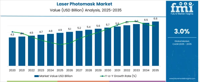
| Metric | Value |
|---|---|
| Laser Photomask Market Estimated Value in (2025 E) | USD 4.9 billion |
| Laser Photomask Market Forecast Value in (2035 F) | USD 6.6 billion |
| Forecast CAGR (2025 to 2035) | 3.0% |
The laser photomask market represents a critical segment within the semiconductor fabrication and microelectronics industry, serving as an essential tool for pattern transfer in chip manufacturing. Within the broader semiconductor equipment sector, it accounts for about 4.9%, supported by ongoing advancements in lithography processes. In the photomask and reticle market, its share is estimated at 6.2%, reflecting reliance on high precision laser-based patterning technologies.
Across the electronics and microcircuitry production space, it holds 3.8%, highlighting its role in enabling compact, high-performance devices. Within the display manufacturing equipment category, it represents 3.5%, driven by demand for advanced panels and OLED displays. In the nanofabrication and MEMS applications market, it secures 3.1%, demonstrating integration in sensors, microfluidics, and emerging nanoscale components. Recent developments in this market have highlighted significant progress in precision, resolution, and efficiency. The adoption of advanced laser writers capable of sub-10 nanometer accuracy has gained traction, addressing next-generation semiconductor requirements.
Multi-beam laser systems and maskless lithography are emerging as groundbreaking approaches, reducing cycle times and enhancing design flexibility. Key players are focusing on collaborative strategies with chipmakers to co-develop photomask solutions optimized for extreme ultraviolet (EUV) and deep ultraviolet (DUV) lithography. Integration of AI-driven defect inspection and repair technologies is improving quality and yield. The investments in materials innovation, including advanced quartz substrates and pellicles, are being prioritized to extend photomask durability and performance. These advancements illustrate how precision engineering and technological innovation are driving the future of the market.
The laser photomask market is experiencing steady expansion supported by the growing demand for advanced semiconductor manufacturing and increasing adoption of photolithography technologies in microelectronics. The rising complexity of integrated circuits and the push toward smaller node sizes have driven investments in high precision photomask production.
Advancements in material engineering, coating technologies, and laser writing equipment have enhanced mask resolution, durability, and defect control. The integration of extreme ultraviolet lithography into high volume manufacturing has further elevated the demand for specialized photomasks with superior optical performance.
Strategic collaborations between semiconductor foundries and photomask manufacturers are reinforcing capacity expansion to meet escalating production requirements. The outlook for the market remains strong as the global electronics industry continues to prioritize miniaturization, performance enhancement, and yield optimization.
The laser photomask market is segmented by photomask type, substrate material, technology, application, end use industry, and geographic regions. By photomask type, laser photomask market is divided into reticle photomasks, master photomasks, and replicated photomasks. In terms of substrate material, laser photomask market is classified into quartz photomasks, soda-lime photomasks, and film photomasks.
Based on technology, laser photomask market is segmented into EUV (extreme ultraviolet) photomasks, DUV (deep ultraviolet) photomasks, Binary photomasks, and Phase shift photomasks. By application, laser photomask market is segmented into semiconductor fabrication, flat panel display manufacturing, MEMS (micro-electromechanical systems), IC packaging, optoelectronics, and other. By end use industry, laser photomask market is segmented into consumer electronics, automotive, healthcare & medical devices, aerospace & defense, telecommunication, and others. Regionally, the laser photomask industry is classified into North America, Latin America, Western Europe, Eastern Europe, Balkan & Baltic Countries, Russia & Belarus, Central Asia, East Asia, South Asia & Pacific, and the Middle East & Africa.
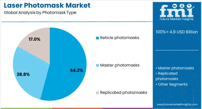
The reticle photomasks segment is projected to hold 54.2% of total market revenue by 2025 within the photomask type category, making it the leading segment. This dominance is driven by their critical role in transferring circuit patterns with high precision in semiconductor manufacturing.
The ability to support advanced lithography nodes and maintain accuracy over multiple exposures has contributed to their sustained demand.
Increasing production of high performance chips for consumer electronics, automotive applications, and data centers is further reinforcing their market leadership.
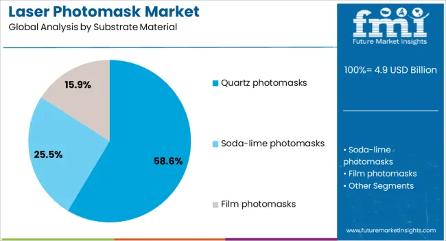
The quartz photomasks segment is expected to account for 58.6% of total revenue by 2025 within the substrate material category, positioning it as the most prominent segment.
This is attributed to quartz’s superior optical transparency, thermal stability, and resistance to radiation damage, which are essential for high precision lithography.
The material’s ability to maintain structural integrity under intense laser exposure has made it the preferred choice for advanced semiconductor manufacturing, especially in processes requiring extreme accuracy.
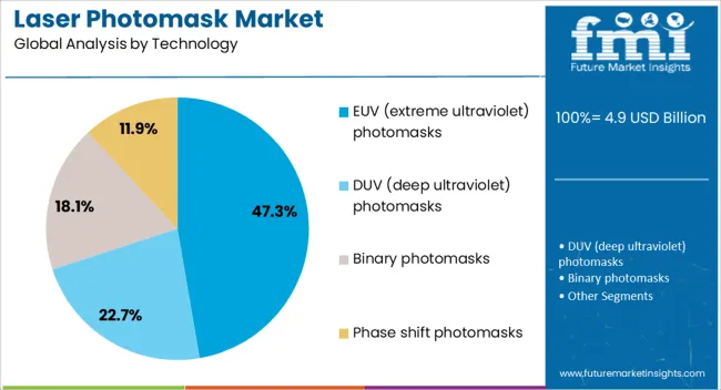
The EUV photomasks segment is anticipated to contribute 47.3% of total revenue by 2025 within the technology category, making it the dominant technology segment. This growth is being driven by the accelerated adoption of extreme ultraviolet lithography in next generation chip fabrication.
EUV photomasks enable the creation of smaller and more complex circuit patterns while improving yield and reducing process steps.
Their role in supporting cutting edge semiconductor nodes has made them indispensable to leading foundries aiming for high performance and energy efficient device production.
The market has gained importance as semiconductor manufacturing and microelectronics industries advance toward finer lithography processes. Photomasks serve as critical templates in circuit patterning, enabling precision in integrated circuits, flat panel displays, MEMS devices, and optoelectronics. Growth has been influenced by increasing semiconductor demand, rising production of consumer electronics, and expansion of data centers. Technological progress in extreme ultraviolet lithography and multi-beam mask writers has created opportunities for high-resolution mask applications. At the same time, cost pressures, complexity of mask design, and stringent quality requirements drive ongoing investments in research, precision equipment, and inspection systems.
Global semiconductor and electronics demand has accelerated the adoption of advanced photomask technologies. As chip architectures become increasingly complex, photomasks designed with high precision and low defect levels are essential for scaling down device nodes. Electronics manufacturing, including smartphones, wearables, and IoT devices, continues to push toward higher density and performance, requiring masks with tighter critical dimension control. Photomasks have become indispensable in enabling rapid production cycles, as lithography remains central to semiconductor fabrication. With AI, 5G, and high-performance computing applications expanding globally, the reliance on photomask solutions in advanced wafer fabrication continues to rise, supporting strong market growth.
Technological advancements in laser photomask systems have strengthened resolution, precision, and efficiency. The shift toward extreme ultraviolet (EUV) lithography has created opportunities for advanced masks capable of supporting smaller process nodes. Multi-beam mask writers and enhanced defect inspection tools are used to ensure pattern fidelity. Automation in mask production and the adoption of sophisticated computational lithography techniques have reduced defect rates and improved turnaround times. Furthermore, hybrid approaches using both electron beam and laser technologies are being explored for cost-effective mask writing. These innovations support continued scaling of semiconductor devices while addressing the industry’s challenges in pattern complexity and accuracy.
While semiconductors remain the largest demand driver, photomasks are increasingly used in flat panel displays, microelectromechanical systems, photonics, and advanced packaging. OLED and LCD display manufacturing rely on high-quality masks for precision patterning, as panel resolution requirements increase. MEMS applications in automotive, medical devices, and sensors also depend on photomasks for consistent and accurate structures. In addition, integrated photonics and advanced interconnect packaging have expanded opportunities for mask suppliers. These new areas of adoption enhance the versatility of laser photomask technologies, allowing the market to diversify its revenue base beyond traditional semiconductor applications.
One of the primary restraints in the laser photomask market is the high cost of mask production and inspection. As device nodes shrink, each mask set becomes more complex and expensive, often reaching millions of dollars for advanced nodes. The supply chain is concentrated, with limited suppliers capable of meeting strict technical and quality requirements, leading to bottlenecks and extended lead times. The geopolitical tensions and trade regulations affecting semiconductor supply chains can disrupt mask availability. Manufacturers face the challenge of balancing cost efficiency with quality assurance while ensuring secure and resilient sourcing of photomasks for global production needs.
| Countries | CAGR |
|---|---|
| China | 4.1% |
| India | 3.8% |
| Germany | 3.5% |
| France | 3.2% |
| UK | 2.9% |
| USA | 2.6% |
| Brazil | 2.3% |
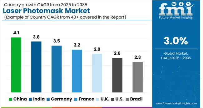
The market is expected to expand at a CAGR of 3.0% from 2025 to 2035, supported by advancements in semiconductor manufacturing and lithography processes. Germany recorded 3.5%, where progress in microelectronics and precision optics sustained demand. India achieved 3.8%, benefiting from growth in chip design and fabrication initiatives. China reached 4.1%, driven by strong investment in semiconductor capacity and localized technology development. The United Kingdom posted 2.9%, with demand tied to research and photonics applications. The United States stood at 2.6%, reflecting adoption within integrated circuit production and innovation in microfabrication. These countries highlight distinct contributions to scaling and innovation in the global Laser Photomask market. This report includes insights on 40+ countries; the top markets are shown here for reference.
China is projected to advance at a CAGR of 4.1%, driven by increasing investments in semiconductor manufacturing, consumer electronics, and integrated circuit design. Domestic demand has been reinforced by large scale government programs supporting self-sufficiency in chip production and photomask fabrication. Major foundries and photomask suppliers are expanding capacity to reduce dependency on imports. Rising applications in flat panel displays, memory devices, and logic ICs further push adoption. Local companies are focusing on high resolution and low defect photomask technologies, supported by R&D collaborations with universities and global suppliers.
India is forecast to grow at a CAGR of 3.8%, supported by rising demand from electronics manufacturing, automotive semiconductors, and telecom sectors. Government backed programs like Make in India and semiconductor policy initiatives encourage photomask usage in chip fabrication and design. While domestic production is limited, collaborations with international suppliers provide access to advanced photomask technologies. Growth is further supported by demand in optoelectronics, MEMS devices, and LED panel manufacturing.
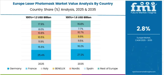
Germany is anticipated to grow at a CAGR of 3.5%, driven by demand from automotive electronics, industrial automation, and advanced microelectronics. Photomask adoption has been reinforced by strong R&D activities and collaboration with European Union programs for semiconductor innovation. German companies emphasize precision, defect free, and reliable photomask production to support domestic chipmaking as well as exports to the broader European region. Use cases extend to sensors, advanced displays, and memory modules.
The United Kingdom is projected to grow at a CAGR of 2.9%, with demand concentrated in research institutions, chip design hubs, and specialty electronics manufacturing. While large scale photomask production is limited, reliance on imports remains high, particularly from East Asia. Domestic companies and universities collaborate to advance photolithography research, focusing on nanotechnology and optoelectronics. Government funding for semiconductor resilience is expected to indirectly support photomask adoption in the coming years.
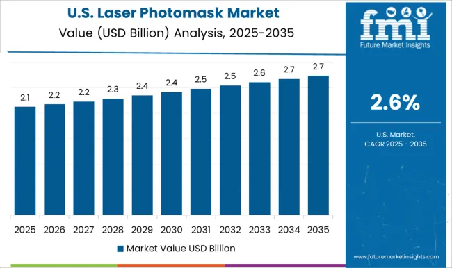
The United States is expected to expand at a CAGR of 2.6%, supported by strong demand from semiconductor fabrication plants, memory device manufacturers, and logic IC developers. Domestic firms dominate global photomask technology, with advanced processes such as EUV photomasks being commercialized by key players. Growth is reinforced by the CHIPS and Science Act, which incentivizes domestic semiconductor production, indirectly boosting photomask adoption. Applications in aerospace, defense electronics, and high performance computing add to market demand.
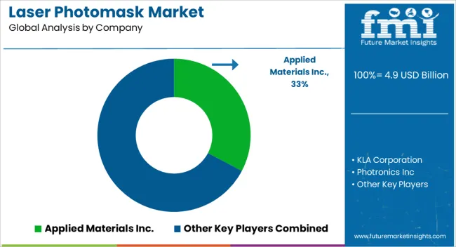
The market features a blend of semiconductor equipment giants, specialized mask producers, and technology innovators that together shape the competitive environment. Applied Materials Inc. leverages its extensive expertise in semiconductor fabrication equipment to integrate photomask solutions with wafer processing technologies, providing end-to-end capabilities to chipmakers. KLA Corporation has established its position by offering advanced metrology and inspection systems, enabling early defect detection and enhancing process control, which is vital for achieving precision in photomask production. Photronics Inc., as one of the largest independent photomask suppliers, operates across diverse applications including integrated circuits, flat panel displays, and memory devices, making it a critical supplier in the global electronics supply chain.
Other contributors to the market include niche photomask providers, regional players, and technology-focused firms that emphasize customized services, innovative mask designs, and cost-effective production methods. Competition is influenced by the demand for smaller node technology, extreme ultraviolet (EUV) mask readiness, and growing adoption of advanced display technologies. Partnerships with semiconductor foundries, continuous R&D investments, and scalable production capacities are shaping long-term competitive advantages, while the rising complexity of semiconductor architectures continues to raise barriers to entry.
| Items | Values |
|---|---|
| Quantitative Units | USD 4.9 billion |
| Photomask Type | Reticle photomasks, Master photomasks, and Replicated photomasks |
| Substrate Material | Quartz photomasks, Soda-lime photomasks, and Film photomasks |
| Technology | EUV (extreme ultraviolet) photomasks, DUV (deep ultraviolet) photomasks, Binary photomasks, and Phase shift photomasks |
| Application | Semiconductor fabrication, Flat panel display manufacturing, MEMS (micro-electromechanical systems), IC packaging, Optoelectronics, and Other |
| End Use Industry | Consumer electronics, Automotive, Healthcare & medical devices, Aerospace & defense, Telecommunication, and Others |
| Regions Covered | North America, Europe, Asia-Pacific, Latin America, Middle East & Africa |
| Country Covered | United States, Canada, Germany, France, United Kingdom, China, Japan, India, Brazil, South Africa |
| Key Companies Profiled | Applied Materials Inc., KLA Corporation, and Photronics Inc |
| Additional Attributes | Dollar sales by photomask type and end-use application, demand dynamics across semiconductor, display, and MEMS manufacturing, regional trends in wafer fab and advanced packaging expansion, innovation in patterning resolution and phase shift technologies, environmental impact of chemical usage and waste management, and emerging use cases in advanced node lithography, microLEDs, and AR/VR displays. |
The global laser photomask market is estimated to be valued at USD 4.9 billion in 2025.
The market size for the laser photomask market is projected to reach USD 6.6 billion by 2035.
The laser photomask market is expected to grow at a 3.0% CAGR between 2025 and 2035.
The key product types in laser photomask market are reticle photomasks, master photomasks and replicated photomasks.
In terms of substrate material, quartz photomasks segment to command 58.6% share in the laser photomask market in 2025.

Full Research Suite comprises of:
Market outlook & trends analysis
Interviews & case studies
Strategic recommendations
Vendor profiles & capabilities analysis
5-year forecasts
8 regions and 60+ country-level data splits
Market segment data splits
12 months of continuous data updates
DELIVERED AS:
PDF EXCEL ONLINE
Laser Transverse Mode Teaching Instrument Market Forecast and Outlook 2025 to 2035
Laser Welding Equipment Market Forecast and Outlook 2025 to 2035
Laser Welding Market Size and Share Forecast Outlook 2025 to 2035
Laser Ablation Systems Market Size and Share Forecast Outlook 2025 to 2035
Laser Measurement Integrating Sphere Market Size and Share Forecast Outlook 2025 to 2035
Laser Safety Cloths Market Size and Share Forecast Outlook 2025 to 2035
Laser Dazzler Market Size and Share Forecast Outlook 2025 to 2035
Laser Cable Marking Market Size and Share Forecast Outlook 2025 to 2035
Laser Cladding Market Size and Share Forecast Outlook 2025 to 2035
Laser Marking Equipment Market Size and Share Forecast Outlook 2025 to 2035
Laser Cutting Machines Market Size and Share Forecast Outlook 2025 to 2035
Laser Wire Marking Systems Market Size and Share Forecast Outlook 2025 to 2035
Laser Measuring Instrument Market Size and Share Forecast Outlook 2025 to 2035
Laser Welding Machine Market Size and Share Forecast Outlook 2025 to 2035
Laser Technology Market Size and Share Forecast Outlook 2025 to 2035
Laser Interferometer Market Size and Share Forecast Outlook 2025 to 2035
The Laser Therapy Devices Market is segmented by Device Type and End User from 2025 to 2035
Laser Safety Glasses Market Growth – Trends & Forecast 2025 to 2035
LASER Light Cables Market Growth – Trends & Forecast 2025 to 2035
Laser Trackers Market - Growth, Demand & Forecast 2025 to 2035

Thank you!
You will receive an email from our Business Development Manager. Please be sure to check your SPAM/JUNK folder too.
Chat With
MaRIA