The microLED photoluminescence inspection system market begins its decade journey from a USD 440.0 million foundation in 2025, setting the stage for substantial expansion ahead. The first half of the decade witnesses steady momentum building, with market value climbing from USD 468.6 million in 2026 to USD 642.0 million by 2030. This initial phase reflects growing microLED adoption across display applications and increasing quality control requirements in semiconductor manufacturing.
The latter half will witness accelerated growth dynamics, propelling the market from USD 683.8 million in 2031 to reach USD 825.9 million by 2035. Dollar additions during 2030-2035 maintain robust progression, with annual increments averaging USD 36.8 million compared to USD 40.4 million in the first phase. This progression represents an 87.7% total value increase over the forecast decade.
Market maturation factors include expanding microLED display production, advanced semiconductor quality requirements, and next-generation inspection technology integration. The 6.5% compound annual growth rate positions participants to capitalize on USD 385.9 million in additional market value creation. This trajectory signals robust opportunities for inspection equipment manufacturers, optical technology providers, and automated testing solution developers across the global electronics manufacturing landscape.
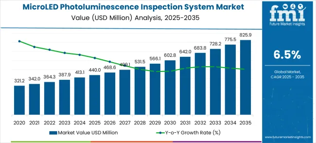
Market expansion unfolds through two distinct growth periods with different technological characteristics for each phase. The 2025-2030 foundation period delivers USD 202.0 million in value additions, representing 45.9% growth from the baseline. Market dynamics during this phase center on microLED technology commercialization, quality control standardization, and inspection system sophistication across manufacturing processes.
The 2030-2035 maturation period generates USD 183.9 million in incremental value, reflecting 28.6% growth from the 2030 position. This phase exhibits mature market characteristics with enhanced competition, advanced inspection integration strategies, and geographic manufacturing expansion initiatives. Dollar contributions shift from foundational technology validation to advanced automated inspection capabilities and next-generation display technology requirements.
Competitive landscape evolution progresses from specialty inspection equipment supply to integrated quality assurance solutions. The first period emphasizes technology validation and manufacturing process optimization. The second period witnesses intensified competition for premium application segments and comprehensive solution development across wafer-level inspection, display manufacturing, and emerging microLED applications.
| Metric | Value |
|---|---|
| Market Value (2025) → | USD 440.0million |
| Market Forecast (2035) ↑ | USD 825.9 million |
| Growth Rate ↑ | 6.5% CAGR |
| Segment Leader → | Floor-standing Type |
| Application Focus ★ | Wafer/ICs |
Market expansion rests on four fundamental shifts driving microLED inspection technology demand acceleration:
The growth faces headwinds from high equipment costs and complex calibration requirements for specialized inspection applications. Traditional optical inspection methods maintain cost advantages for less demanding quality control applications. Technical complexity creates adoption barriers for smaller manufacturing operations with limited technical expertise and capital resources.
Primary Classification: System Type Distribution
Secondary Breakdown: Application Categories
Geographic Segmentation: Regional Market Distribution
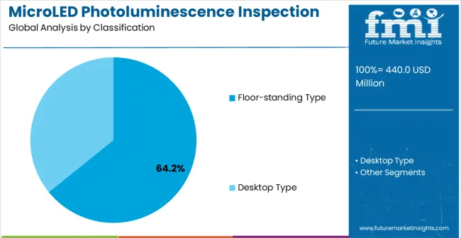
Market Position: Floor-standing photoluminescence inspection systems establish clear market leadership through comprehensive measurement capabilities and advanced automation features essential for high-volume manufacturing environments. Precision optical components and sophisticated measurement algorithms enable accurate evaluation of microLED performance characteristics across wide wavelength ranges. Automated sample handling systems facilitate high-throughput inspection protocols required for commercial microLED production scaling.
Value Drivers: Advanced optical design incorporating high-resolution imaging systems and sensitive detection capabilities enables precise measurement of photoluminescence intensity, wavelength distribution, and spatial uniformity. Automated data analysis software provides comprehensive reporting and statistical analysis supporting quality control decision-making and process optimization. Integration capabilities enable connection with manufacturing execution systems for real-time quality monitoring and feedback control.
Competitive Advantages: Floor-standing systems offer superior measurement accuracy and repeatability compared to desktop alternatives through enhanced optical isolation and environmental control capabilities. Automation features reduce operator dependency while improving measurement consistency and throughput for high-volume production environments. Modular design enables flexible configuration accommodating diverse microLED device types and measurement requirements.
Market Challenges: High capital investment requirements create adoption barriers for smaller manufacturing operations and research institutions with limited budgets. Complex installation and calibration procedures require specialized technical expertise and extended setup timeframes. Maintenance costs include regular calibration services and optical component replacement affecting total cost of ownership.
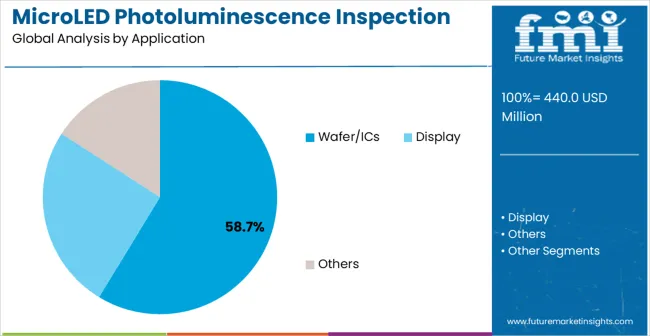
Strategic Market Importance: Wafer-level inspection represents the primary demand driver for photoluminescence systems across semiconductor manufacturing processes incorporating LED structures. Comprehensive wafer-scale evaluation enables identification of performance variations and defect patterns affecting device yield and reliability. Quality control protocols require systematic inspection of LED characteristics including efficiency, wavelength uniformity, and spatial distribution across entire wafer surfaces.
Market Dynamics Q&A:
Business Logic: Semiconductor manufacturers prioritize yield optimization and quality control, making comprehensive wafer-level inspection essential for competitive manufacturing economics and customer satisfaction. Early defect identification reduces manufacturing costs through process optimization and prevents costly field failures. Investment justification occurs through improved manufacturing yield and reduced warranty claims over product lifecycle.
Forward-looking Implications: Integration of LED structures in advanced semiconductor devices creates expanding opportunities for wafer-level photoluminescence inspection across multiple technology segments. Autonomous vehicle electronics demand exceptional reliability requiring comprehensive inspection protocols for LED-based sensor and display systems. Quantum computing and photonic integrated circuits may create new application opportunities for specialized optical inspection technologies.
Growth Accelerators
MicroLED technology commercialization drives increasing demand for specialized inspection equipment supporting display manufacturing and semiconductor applications. Quality control enhancement mandates comprehensive optical inspection systems preventing defective devices from reaching final assembly and customer delivery. Manufacturing yield optimization requires advanced inspection capabilities enabling real-time process monitoring and feedback control for production efficiency improvement. Display application expansion across automotive, wearable, and consumer electronics creates demand for microLED quality control technologies.
High equipment costs create adoption barriers for smaller manufacturing operations and research institutions requiring significant capital investment justification. Technical complexity necessitates specialized operator training and maintenance expertise increasing operational costs and implementation challenges. Limited standardization across different microLED technologies creates compatibility issues requiring customized inspection solutions. Competitive pressure from alternative display technologies may limit microLED adoption affecting long-term inspection equipment demand.
Artificial intelligence integration enables automated defect classification and process optimization through machine learning algorithms analyzing inspection data patterns. Multi-wavelength inspection capabilities provide comprehensive evaluation of microLED performance characteristics across visible and infrared spectral ranges. Inline inspection systems facilitate real-time quality monitoring during manufacturing processes enabling immediate feedback and process adjustment. Cloud-based data analytics enable predictive maintenance and performance optimization across multiple manufacturing facilities and equipment installations.
| Country | CAGR (%) |
|---|---|
| China | 8.8 |
| India | 8.1 |
| Germany | 7.5 |
| Brazil | 6.8 |
| United States | 6.2 |
| United Kingdom | 5.5 |
| Japan | 4.9 |
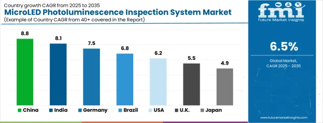
Global market dynamics reveal distinct performance tiers reflecting regional microLED development priorities and manufacturing investment strategies. High-Growth Markets including China (8.8% CAGR) and India (8.1% CAGR) demonstrate aggressive microLED manufacturing capacity expansion with comprehensive quality control system adoption. Technology Leaders such as Germany (7.5% CAGR) represent European precision engineering excellence with advanced optical inspection capabilities. Steady Performers including Brazil (6.8% CAGR) and the United States (6.2% CAGR) show consistent growth aligned with display technology advancement and semiconductor manufacturing expansion. Mature Markets including the United Kingdom (5.5% CAGR) and Japan (4.9% CAGR) display moderate growth rates reflecting established manufacturing infrastructure with advanced inspection technology focus.
The report covers an in-depth analysis of 40+ countries with top-performing countries are highlighted below.
China establishes market leadership through massive display manufacturing capacity and comprehensive microLED technology development initiatives. The 8.8% CAGR reflects unprecedented investment in next-generation display technologies supporting domestic consumer electronics industry and export market competitiveness. Government support for advanced display technologies creates demand for sophisticated inspection equipment and quality control systems.
Display manufacturing capacity exceeding 70% of global production requires comprehensive quality control systems and inspection equipment across multiple facility locations. MicroLED technology development programs supported by government funding and industry collaboration create expanding demand for advanced testing capabilities and measurement systems. Consumer electronics manufacturing leadership necessitates cutting-edge display technologies and associated quality control systems ensuring international competitiveness.
Strategic market indicators include display manufacturing investment exceeding USD 50 billion annually requiring comprehensive inspection equipment deployment. Government technology development programs promote domestic microLED industry advancement and manufacturing capability development through targeted investment initiatives. Export quality requirements drive adoption of international standard inspection systems and quality assurance protocols supporting global market competitiveness and customer satisfaction requirements.
Strategic Market Indicators:
India demonstrates robust growth potential through expanding electronics manufacturing ecosystem and government promotion of domestic display technology development initiatives. The 8.1% CAGR reflects increasing manufacturing sophistication and quality control requirements supporting Make in India programs and foreign investment attraction. Technology transfer partnerships create opportunities for advanced inspection equipment adoption and local capability development across multiple manufacturing sectors.
Electronics manufacturing growth exceeding 20% annually creates expanding demand for advanced display technologies and comprehensive quality control systems. Government Production Linked Incentive schemes promote domestic display manufacturing requiring inspection equipment and quality assurance capabilities supporting local production scaling. Foreign investment in advanced manufacturing brings international quality standards and inspection technology requirements to domestic facilities.
Market development focuses on skilled workforce development programs including training for advanced manufacturing techniques and quality control procedures supporting inspection equipment adoption. Export market development creates opportunities for high-quality display production requiring advanced inspection capabilities and international quality certification. Regional manufacturing hub development consistent demand growth across electronics production facilities and technology advancement initiatives supporting long-term market expansion.
Market Intelligence Brief:
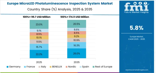
Germany maintains technology leadership through precision optical equipment manufacturing and comprehensive inspection system development capabilities. The 7.5% CAGR reflects established engineering excellence with continuous advancement in optical measurement technologies and quality control systems. Automotive and industrial applications create consistent demand for high-performance inspection equipment and advanced quality assurance systems across multiple technology segments.
Optical equipment exports exceed EUR 25 billion annually including specialized inspection systems and measurement technologies supporting global manufacturing requirements. Research and development investment in optical technologies leads global innovation advancement in inspection equipment and quality control systems. Quality standard development influences international manufacturing practices and inspection system requirements across multiple industries.
Engineering services sector creates specialized inspection equipment development and optimization capabilities for microLED applications supporting customer requirements. Automotive industry requirements drive advanced display technology adoption necessitating sophisticated inspection capabilities and quality control systems. Manufacturing precision culture drives continuous improvement in inspection technology accuracy and reliability exceeding international benchmark standards supporting German technological leadership and global competitiveness.
Performance Metrics:
Brazil represents emerging market growth potential with a 6.8% CAGR through expanding electronics manufacturing and government initiatives supporting domestic technology development. Industrial development programs create opportunities for advanced manufacturing technology adoption including inspection equipment and quality control systems supporting regional electronics production requirements across multiple facility locations.
Electronics manufacturing sector contributes increasing economic value with advanced technology requirements and quality control needs supporting industrial development objectives. Government industrial development programs promote domestic electronics manufacturing requiring comprehensive inspection capabilities and quality assurance systems. Regional trade agreements facilitate technology transfer and equipment importation supporting advanced manufacturing development.
Foreign investment brings international quality standards and advanced inspection technology requirements to domestic manufacturing operations and facilities. Infrastructure development supports industrial electronics production and quality control system implementation across manufacturing facilities and industrial regions. Market development centers on technology localization initiatives reducing import dependency while building domestic technical capabilities. Export market development creates opportunities for regional competitiveness through advanced manufacturing technologies and comprehensive quality control system implementation supporting long-term growth.
Strategic Market Considerations:
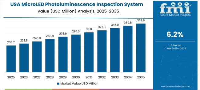
The United States demonstrates steady growth with a 6.2% CAGR through advanced display technology research and semiconductor manufacturing innovation coupled with federal investment in advanced manufacturing capabilities. Silicon Valley technology ecosystem combined with government research funding creates demand for cutting-edge inspection equipment and quality control systems across multiple technology sectors.
Advanced display technology research and development leadership creates demand for sophisticated inspection equipment and measurement systems supporting innovation programs. Semiconductor manufacturing excellence requires comprehensive quality control systems and inspection equipment for advanced device production and technology development. Federal research investment exceeds USD 10 billion annually supporting advanced manufacturing technologies including inspection equipment development.
Defense and aerospace applications require ultra-high reliability display technologies necessitating comprehensive inspection capabilities and quality assurance protocols. University research partnerships advance inspection technology development through collaborative programs and technology transfer initiatives supporting commercial equipment advancement. Manufacturing competitiveness initiatives encourage investment in advanced inspection technologies supporting domestic production capabilities and technological leadership in global markets.
Market Development Focus:
The United Kingdom demonstrates focused growth with a 5.5% CAGR through advanced materials research and optical technology development supported by world-class universities and government innovation programs. Brexit-related technology strategy initiatives promote domestic manufacturing capabilities while maintaining strong international research collaboration networks supporting inspection equipment development and commercialization.
Advanced optical research programs position UK leadership in next-generation inspection technology development and measurement system advancement. Government innovation funding exceeds GBP 1.5 billion annually supporting advanced manufacturing technology development including inspection equipment and quality control systems. University partnerships create comprehensive technology transfer opportunities for inspection equipment advancement and commercial application development.
Aerospace and defense applications require ultra-high reliability components necessitating advanced inspection capabilities and quality control systems. Export market specialization necessitates international quality standard compliance and advanced inspection equipment certification for global market competitiveness. Innovation ecosystem combines academic excellence with industrial application creating opportunities for breakthrough inspection technology development supporting UK technological leadership and international market positioning across multiple sectors.
Innovation Indicators:
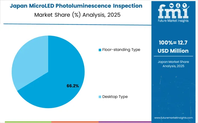
Japan maintains established market position with a 4.9% CAGR through precision manufacturing excellence and advanced optical technology development capabilities. Legacy semiconductor and display industry expertise combined with continuous innovation creates consistent demand for sophisticated inspection equipment and quality control systems across multiple high-technology application segments.
Display technology manufacturing excellence creates consistent demand for advanced inspection equipment and quality control systems across multiple application segments. Optical equipment manufacturing leadership provides comprehensive inspection system capabilities and advanced measurement technology development supporting domestic and international markets. Semiconductor industry expertise drives continuous advancement in inspection technology and quality control system optimization.
Automotive electronics leadership requires exceptional quality control systems and inspection capabilities supporting advanced display integration and performance requirements. International technology export necessitates superior inspection equipment quality and performance characteristics supporting Japanese manufacturing competitiveness and global market leadership. Manufacturing precision culture drives continuous quality improvement and process optimization for inspection system reliability and accuracy supporting technological excellence and international competitiveness.
Technology Leadership Aspects:
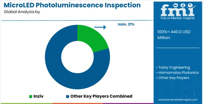
Market structure reflects moderate concentration with established optical equipment manufacturers maintaining significant positions while specialized technology providers serve specific application segments. Competition emphasizes technological innovation, measurement accuracy, and comprehensive solution integration capabilities across diverse microLED manufacturing requirements. Industry dynamics favor companies combining advanced optical design expertise with sophisticated software capabilities, automation features, and global service networks enabling comprehensive customer support.
The competitive environment increasingly focuses on differentiation through advanced measurement capabilities, automated data analysis, and integrated manufacturing system connectivity. Market leaders invest heavily in research and development to maintain technological advantages while emerging players leverage specialization and regional expertise to capture specific market segments. Strategic partnerships between equipment manufacturers and microLED producers drive collaborative innovation and application-specific solution development.
Tier 1 - Global Optical Technology Leaders: Companies like Hamamatsu Photonics and Horiba dominate through comprehensive photoluminescence measurement portfolios, global service networks, and extensive research and development capabilities spanning decades of optical expertise. Competitive advantages include proven optical design excellence, established customer relationships across semiconductor and display industries, and integrated solution capabilities spanning multiple inspection applications. These market leaders leverage economies of scale, comprehensive intellectual property portfolios, and global manufacturing capabilities to maintain premium market positioning.
Tier 2 - Specialized Inspection Providers: Organizations including Inziv and Toray Engineering focus on specific microLED applications through specialized expertise and targeted market development strategies. Competitive advantages include deep application-specific knowledge, flexible customization capabilities, and regional market specialization enabling responsive technical support and rapid system optimization. These companies often pioneer innovative approaches and serve as technology incubators for emerging measurement techniques. Their agile business models enable faster adaptation to evolving microLED requirements and emerging technology trends compared to larger competitors. Strategic focus on niche applications allows for premium pricing strategies and strong customer loyalty through specialized technical expertise and personalized service offerings.
Tier 3 - Regional and Component Specialists: Companies including ELP and AlphaBetter serve specific geographic markets through cost-competitive solutions and specialized measurement capabilities tailored to local requirements. Competitive advantages include intimate regional market knowledge, flexible production capacity, and close partnership relationships with microLED manufacturers and research institutions enabling collaborative development programs and customized solutions. These players often serve as crucial supply chain partners for local manufacturers seeking cost-effective inspection solutions with responsive technical support. Their market strategies emphasize value engineering and rapid deployment capabilities, providing essential market access for emerging microLED manufacturers and research organizations with limited capital budgets.
| Item | Value |
|---|---|
| Quantitative Units | USD 825.9 million |
| System Type | Floor-standing Type, Desktop Type, Others |
| Application | Wafer/ICs, Display, Others |
| Regions Covered | North America, Latin America, Europe, East Asia, South Asia & Pacific, Middle East & Africa |
| Countries Covered | United States, Canada, Mexico, Germany, United Kingdom, France, Italy, Spain, Nordic, BENELUX, China, Japan, South Korea, India, ASEAN, Australia, New Zealand, Brazil, Chile, Kingdom of Saudi Arabia, GCC Countries, Turkey, South Africa |
| Key Companies Profiled | Inziv, Toray Engineering, Hamamatsu Photonics, ANI, ELP, EtaMax, Horiba, Southport Corporation, AlphaBetter |
| Additional Attributes | Dollar sales by system type categories, regional demand trends across North America, Europe, and Asia-Pacific, competitive landscape analysis, adoption patterns across microLED sectors, integration with manufacturing systems, optical technology innovations, quality control standards |
The global microled photoluminescence inspection system market is estimated to be valued at USD 440.0 million in 2025.
The market size for the microled photoluminescence inspection system market is projected to reach USD 825.9 million by 2035.
The microled photoluminescence inspection system market is expected to grow at a 6.5% CAGR between 2025 and 2035.
The key product types in microled photoluminescence inspection system market are floor-standing type and desktop type.
In terms of application, wafer/ics segment to command 58.7% share in the microled photoluminescence inspection system market in 2025.
Our Research Products

The "Full Research Suite" delivers actionable market intel, deep dives on markets or technologies, so clients act faster, cut risk, and unlock growth.

The Leaderboard benchmarks and ranks top vendors, classifying them as Established Leaders, Leading Challengers, or Disruptors & Challengers.

Locates where complements amplify value and substitutes erode it, forecasting net impact by horizon

We deliver granular, decision-grade intel: market sizing, 5-year forecasts, pricing, adoption, usage, revenue, and operational KPIs—plus competitor tracking, regulation, and value chains—across 60 countries broadly.

Spot the shifts before they hit your P&L. We track inflection points, adoption curves, pricing moves, and ecosystem plays to show where demand is heading, why it is changing, and what to do next across high-growth markets and disruptive tech

Real-time reads of user behavior. We track shifting priorities, perceptions of today’s and next-gen services, and provider experience, then pace how fast tech moves from trial to adoption, blending buyer, consumer, and channel inputs with social signals (#WhySwitch, #UX).

Partner with our analyst team to build a custom report designed around your business priorities. From analysing market trends to assessing competitors or crafting bespoke datasets, we tailor insights to your needs.
Supplier Intelligence
Discovery & Profiling
Capacity & Footprint
Performance & Risk
Compliance & Governance
Commercial Readiness
Who Supplies Whom
Scorecards & Shortlists
Playbooks & Docs
Category Intelligence
Definition & Scope
Demand & Use Cases
Cost Drivers
Market Structure
Supply Chain Map
Trade & Policy
Operating Norms
Deliverables
Buyer Intelligence
Account Basics
Spend & Scope
Procurement Model
Vendor Requirements
Terms & Policies
Entry Strategy
Pain Points & Triggers
Outputs
Pricing Analysis
Benchmarks
Trends
Should-Cost
Indexation
Landed Cost
Commercial Terms
Deliverables
Brand Analysis
Positioning & Value Prop
Share & Presence
Customer Evidence
Go-to-Market
Digital & Reputation
Compliance & Trust
KPIs & Gaps
Outputs
Full Research Suite comprises of:
Market outlook & trends analysis
Interviews & case studies
Strategic recommendations
Vendor profiles & capabilities analysis
5-year forecasts
8 regions and 60+ country-level data splits
Market segment data splits
12 months of continuous data updates
DELIVERED AS:
PDF EXCEL ONLINE
Bar Inspection System Market Size and Share Forecast Outlook 2025 to 2035
Tire Inspection System Market - Outlook 2025 to 2035
Packaging Inspection Systems Market Size and Share Forecast Outlook 2025 to 2035
Semiconductor Inspection System Market Size and Share Forecast Outlook 2025 to 2035
Medication Pouch Inspection Systems Market Analysis and Trends 2025 to 2035
Automated Optical Inspection System Market Report - Trends & Forecast 2024 to 2034
Inspection Drone in Oil and Gas Market Size and Share Forecast Outlook 2025 to 2035
Inspection Management Software Market Size and Share Forecast Outlook 2025 to 2035
Inspection Robots Market Size and Share Forecast Outlook 2025 to 2035
System-On-Package Market Size and Share Forecast Outlook 2025 to 2035
Inspection and Inventory Labels Market Size and Share Forecast Outlook 2025 to 2035
Systems Administration Management Tools Market Size and Share Forecast Outlook 2025 to 2035
Inspection Lighting Fixture Market Size and Share Forecast Outlook 2025 to 2035
Inspection & Weighing Machine Industry Analysis in ASEAN and Gulf Countries Analysis - Size, Share, and Forecast 2025 to 2035
Systemic Sclerosis Treatment Market - Trends & Forecast 2025 to 2035
System on Module Market Growth – Trends & Forecast 2025 to 2035
Examining Market Share Trends in Inspection and Inventory Labels
Inspection Machines Market Growth – Trends & Forecast 2025 to 2035
SLE Drugs Market Insights - Growth & Forecast 2025 to 2035
Systemic Mastocytosis Treatment Market

Thank you!
You will receive an email from our Business Development Manager. Please be sure to check your SPAM/JUNK folder too.
Chat With
MaRIA