- Market Size (2026)
- USD 11.8 Bn
- Forecast (2036)
- USD 38.7 Bn
- CAGR (2026 to 2036)
- 12.6%
How big is Sputtering Deposition Equipment Market in 2026?
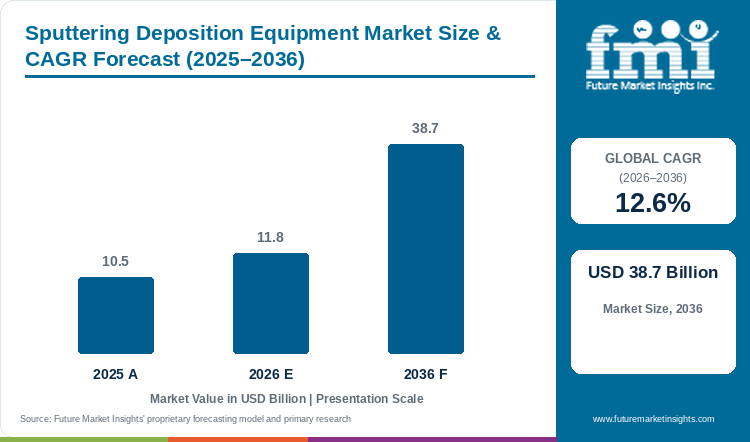
Demand for sputtering deposition equipment is projected to expand at 12.6% CAGR between 2026 and 2036. Industry value grows from USD 10.5 billion in 2025 to USD 11.8 billion in 2026 and is projected to reach USD 38.7 billion by 2036.
Sputtering deposition equipment market is estimated at USD 11.8 billion in 2026, against USD 10.5 billion in 2025, and will reach USD 38.7 billion by 2036 at 12.6% CAGR. As per FMI, value added after 2026 will be USD 26.9 billion, taking the market to 3.3 times its 2026 size. Demand is driven by logic, semiconductor memory and advanced packaging plants adding metal, barrier, contact and seed layers. World Semiconductor Trade Statistics reported USD 795.6 billion in semiconductor sales during 2025, up 26.2% from 2024.[1] Higher chip output adds deposition steps before wafers and packages can move to testing. The U.S. Government Accountability Office reported 49 funded semiconductor projects across 24 companies by August 2026, with USD 13.1 billion already disbursed.[2] The 300 mm advanced fab wafer category will hold 38.3% of wafer size compatibility demand in 2026, as automated fabs add qualified chambers beside existing process lines.
Key Market Trends & Insights
- By wafer size compatibility, 300 mm advanced fab wafers led with 38.3% share in 2026, supported by automated handling and higher die output.
- By process node, sub-5 nm nodes accounted for 50.2% of demand in 2026 as smaller devices requires tighter interconnect and barrier films.
- By system architecture, automated vacuum cluster tools represented 42.6% in 2026 because integrated transfer reduces atmospheric exposure between process steps.
- By end user tier, integrated device manufacturers held 40.7% share in 2026, owing to direct investment in owned logic, memory and power fabs.
Regional Highlights
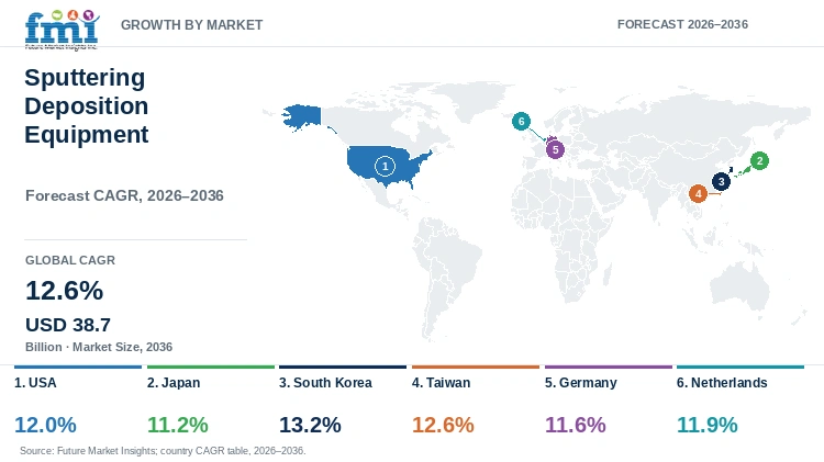
- Fastest-growing profiled country: South Korea (13.2% CAGR, 2026 to 2036).
- Taiwan (12.6%) and the USA (12.0%) follow, while Japan records the lowest profiled CAGR at 11.2%.
Market Size & Forecast
Table 1: Market Size and Forecast for the Sputtering Deposition Equipment Market (USD billion and percentage), 2025 to 2036
| Metric | Value |
|---|---|
| 2025 Market Size | USD 10.5 billion |
| Estimated Market Size in 2026 | USD 11.8 billion |
| Projected Market Size by 2036 | USD 38.7 billion |
| CAGR, 2026 to 2036 | 12.6% |
| Added Revenue, 2026 to 2036 | USD 26.9 billion |
| Market Expansion Multiple | 3.3x |
Equipment orders do not start at the same time as a fab announcement. A production line first moves through tool installation, process integration and customer qualification. Federal program reviews indicate that while awardees completed required milestones by their due dates, certain facility commissioning phases remained behind anticipated schedules. Delays at this stage can move chamber shipment and customer acceptance into a later quarter. In May 2026, Applied Materials agreed to acquire NEXX for adding large-area deposition equipment used in advanced packaging.[3] Panel formats can reach 510 by 515 millimeters or more, due to which film uniformity becomes harder to hold over the full surface. As noted by FMI, fab construction opens the order opportunity, but qualification decides when a chamber enters regular production.
Fab Investment and Equipment Readiness
Fab announcements alone does not explain the complete demand for sputtering deposition equipment. Equipment orders rise when a project reaches installation, process integration and customer qualification. The indicators below connect semiconductor sales, funded projects, panel size and country programs with the stages that create equipment demand. Reporting years are different and the indicators do not represent global market share.
Table 2: Fab Investment and Equipment Readiness Indicators for the Sputtering Deposition Equipment Market (USD billion, projects, companies, millimeters, and percentages), mixed reporting years from 2025 to 2026
| Indicator | Data Point | Why It Matters | Source |
|---|---|---|---|
| Global semiconductor sales | USD 795.6 billion in 2025; 26.2% annual increase | Higher chip sales supports output and capacity requiring additional deposition steps. | [1] |
| U.S. funded fab projects | 49 projects across 24 companies; USD 13.1 billion disbursed by April 2026 | Funded construction creates equipment-installation opportunities before commercial production. | [2] |
| Advanced packaging panel size | 510 by 515 millimeters or more | Larger substrates require wider-area deposition and film-uniformity control. | [3] |
| Taiwan public program | Approximately USD 9.5 billion through 2033 | Shared facilities and pilot production can support equipment testing and customer verification. | [13] |
| Leading wafer category | 300 mm advanced fab wafers at 38.3% in 2026 | Established automation and process recipes supports chamber additions during fab expansion. | FMI estimate |
Analyst Perspective
“More metal layers will keep deposition orders rising faster than wafer starts through 2036. Panel packaging adds new demand, but slow qualification will continue moving some orders between years.”
- Nikhil Kaitwade, Principal Consultant, Future Market Insights.
How is the sputtering deposition equipment market segmented?
Sputtering deposition equipment market is segmented by four primary commercial axes and region: wafer size compatibility, process node, system architecture, end user tier, and region. In 2026, 300 mm wafers are projected at 38.3%, sub-5 nm nodes at 50.2%, cluster tools at 42.6%, and IDMs at 40.7%.
By wafer size compatibility: 300 mm advanced fab wafers, 200 mm legacy fab wafers, and compound semiconductor substrates (SiC/GaN).
By process node: sub-5 nm nodes, 7 nm to 28 nm nodes, and legacy power and discrete nodes.
By system architecture: automated vacuum cluster tools, in-line track systems, single-wafer processing chambers, and batch deposition modules.
By end user tier: integrated device manufacturers, pure-play foundries, OSAT and advanced packaging houses, and research and pilot-line facilities.
By region: North America, Latin America, Western Europe, Eastern Europe, East Asia, South Asia and Pacific, and Middle East and Africa.
Why do 300 mm wafers retain a notable compatibility share?
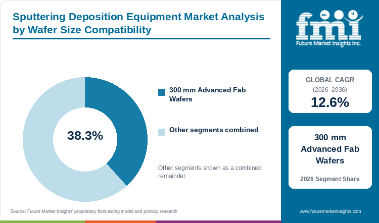
In 2026, 300 mm advanced fab wafers are projected to account for 38.3% of compatibility demand, supported by automated high-volume fabs.
Table 3: Wafer Size Compatibility Share for the Sputtering Deposition Equipment Market (percentage share), 2026
| Wafer Size Compatibility | Share (2026) |
|---|---|
| 300 mm Advanced Fab Wafers | 38.3% |
| Other Segments Combined | 61.7%* |
| Total | 100.0% |
*Calculated as the balance remaining after deducting the leading segment's reported share from 100.0%.
Table 4: Wafer Size Compatibility Leadership and Market Growth for the Sputtering Deposition Equipment Market (segment and CAGR percentage), 2026 to 2036
| Metric | Value |
|---|---|
| Global CAGR (2026 to 2036) | 12.6% |
| Leading Segment | 300 mm Advanced Fab Wafers |
The 300 mm advanced fab wafer category takes 38.3% of wafer size compatibility demand in 2026. Demand is driven by automated fabs using established wafer processing equipment and approved deposition recipes. A chamber added beside a running 300 mm line can use similar wafer transfer and process controls, reducing the work needed before production. In April 2026, SEMI projected worldwide 300mm fab equipment spending to increase 18% to USD 133 billion in 2026, driven by memory and leading-edge logic additions.[4] As per the analysis from FMI, expansion of 300 mm logic, memory and packaging lines will keep this category ahead through the forecast period.
- 300 mm advanced fab wafers account for 38.3% of compatibility demand in 2026, supported by established automated wafer handling and higher die output.
- SEMI projected in April 2026 that global 300mm fab equipment spending will reach USD 133 billion in 2026, reflecting double-digit capacity additions across automated logic and memory facilities.
What supports sub-5 nm nodes as the preferred process category?
By process node, sub-5 nm nodes are estimated to hold 50.2% in 2026, owing to tighter film-control requirements.
Sub-5 nm nodes account for 50.2% of process node demand in 2026. Smaller devices use more interconnect, barrier and contact films alongside complementary atomic layer deposition steps, and every layer needs tighter thickness and resistance control. In April 2026, Applied Materials introduced deposition systems for angstrom-era logic chips.[5] The systems are directed towards wiring and contact structures used when dimensions continue to shrink. According to FMI, additional material layers will support higher deposition equipment demand from advanced logic plants.
- Sub-5 nm nodes account for 50.2% of process node demand in 2026, reflecting the need for denser interconnect, barrier, and contact layers per device.
- Applied Materials introduced new deposition systems for angstrom-era logic chips in April 2026, linking materials control with next-node production.
How are automated cluster tools gaining use in production fabs?
Automated vacuum cluster tools are set to lead system architecture with 42.6% share in 2026, enabled by contamination-controlled transfer.
Automated vacuum cluster tools hold 42.6% of system architecture demand in 2026. These tools combine wafer cleaning, deposition and transfer inside one vacuum environment. Atmospheric breaks are reduced, due to which particles and surface changes can be controlled between sequential steps. Fabs also use one cluster for barrier, seed and related metal films instead of moving wafers between separate semiconductor manufacturing equipment platforms. FMI data suggests that integrated transfer and repeat process control will keep cluster tools as the preferred architecture during the forecast period.
- Automated vacuum cluster tools account for 42.6% of architecture demand in 2026, enabled by vacuum-integrated transfer between sequential deposition steps.
- Integrated chambers reduce atmospheric breaks between cleaning, barrier deposition, seed deposition, and metrology steps.
Why do IDMs anchor sputtering equipment purchasing decisions?
Integrated device manufacturers are projected to hold 40.7% of end-user demand in 2026, underpinned by direct fab ownership.
Integrated device manufacturers account for 40.7% of end user demand in 2026. IDMs own logic, memory, silicon carbide power devices, and specialist semiconductor plants, so equipment orders are placed directly under their capital programs. Industry data from the Semiconductor Industry Association indicates that major manufacturers directed over USD 40 billion in annual capital expenditures toward owned fabrication lines, sustaining dedicated equipment procurement.[6] Many projects cover owned production and packaging facilities requiring deposition equipment before volume output. FMI research indicates that direct fab ownership will continue supporting the IDM share through 2036.
- Integrated device manufacturers account for 40.7% of end-user demand in 2026, underpinned by extensive capital programs spanning logic, memory, power, and specialist devices.
- Industry data indicates that integrated device manufacturers invested over USD 40 billion in fab capital expenditures in 2025 across logic, memory, and power platforms.
What are the drivers, restraints, and opportunities in the sputtering deposition equipment market?
In the sputtering deposition equipment market, fab construction is the key driver, long qualification is the key restraint, and advanced packaging is the key opportunity.
- Driver: New logic, memory, power, and packaging capacity expands the installed requirement for thin-film deposition tools.
- Restraint: Process qualification, export controls, and long fab schedules can defer chamber acceptance and revenue timing.
- Opportunity: Advanced packaging and compound semiconductors need sputtered barrier, seed, adhesion, and electrode films.
Fab Capacity Expands Tool Demand
New semiconductor fabs require sputtering deposition equipment before commercial production starts. In April 2026, SEMI reported that global semiconductor equipment billings reached USD 135 billion in 2025, driven by a 12% increase in wafer processing tool shipments as fabs expanded front-end capacity.[7] Each production line needs high-purity sputtering targets, vacuum transfer and process monitoring systems. Equipment is first installed for process development and more chambers are added when wafer output increases. An FMI analyst notes that funded fab projects will support equipment orders during installation and later capacity expansion.
Qualification Delays Equipment Acceptance
Long qualification period is one of the primary factors restraining the sputtering deposition equipment market. A chamber has to meet film thickness, resistance, particle, stress and step-coverage limits on the customer wafer. In March 2026, the National Institute of Standards and Technology noted that establishing atomic-level thickness uniformity and interface limits on 300 mm wafers requires extensive reference metrology before tools are certified for production.[8] A change in target material or device structure can require another recipe test for specialized thin film coatings. Fabs will not release the tool for regular production until process stability and yield are confirmed. This can delay customer acceptance and may hamper sputtering deposition equipment market growth.
Advanced Packaging Opens New Routes
Advanced packaging is creating new applications for sputtering deposition equipment. Barrier and seed films are deposited before electroplating, redistribution and interconnect formation, often integrated with back grinding system workflows for ultra-thin dies. Larger wafers and panels need equipment which can hold film thickness over a wider surface. In January 2025, the U.S. Department of Commerce awarded USD 300 million under the National Advanced Packaging Manufacturing Program to advance glass-substrate and panel-level packaging technologies, including funding for Applied Materials.[9] Heterogeneous integration and panel-level packaging is expected to create growth opportunities for sputtering deposition equipment manufacturers.
Which country CAGRs are profiled in the sputtering deposition equipment market?
Table 5: Country CAGR Comparison for the Sputtering Deposition Equipment Market (CAGR percentage), 2026 to 2036
| Country | CAGR |
|---|---|
| USA | 12.0% |
| Japan | 11.2% |
| South Korea | 13.2% |
| Taiwan | 12.6% |
| Germany | 11.6% |
| Netherlands | 11.9% |
How do country-level CAGRs compare in the sputtering deposition equipment market?
Country demand is divided between large semiconductor production bases and equipment-led European markets. South Korea at 13.2% CAGR and Taiwan at 12.6% will grow through memory, foundry and advanced packaging investment. The USA at 12.0% is adding logic, memory and packaging facilities under funded semiconductor programs. Japan at 11.2% connects new logic production with domestic materials and equipment suppliers. Germany and the Netherlands will receive selective demand from specialist production, pilot lines and semiconductor equipment development.
In the FMI report, South Korea and Taiwan record stronger growth because both countries combine high wafer output with advanced packaging activity. Germany and the Netherlands grow through research, equipment development and high-mix production, rather than comparable wafer volume.
- USA demand follows awarded fab, memory, and packaging projects under federal semiconductor programs.
- Japan connects next-generation logic investment with a domestic equipment and materials supply base.
- South Korea remains tied to HBM, DRAM, NAND, foundry, and cluster development.
- Taiwan combines front-end fabrication, advanced packaging, and equipment-localization programs.
- Germany uses microelectronics research and production to support industrial, automotive, and power-device demand.
- Netherlands demand is linked to its semiconductor equipment ecosystem and targeted 2035 investment plan.
Full report country CAGRs cover: North America; Latin America; Western Europe; Eastern Europe; East Asia; South Asia and Pacific; Middle East and Africa.
Country-wise Analysis
- The USA sputtering deposition equipment market is forecast to rise at 12.0% CAGR through 2036. Demand is driven by construction of logic, memory and packaging facilities, complementing chemical vapor deposition installations. In December 2025, the U.S. Government Accountability Office reported USD 30.9 billion in direct awards and USD 5.5 billion in loans for 40 projects.[10] Nearly 40% of projects are intended for leading-edge logic production. Each new fab needs PVD systems during equipment installation and adds more chambers when output expands. Project milestones continue through 2033, so changes in construction schedule can move orders between years. Domestic wafer and packaging capacity is expected to support equipment demand in the USA.
- Japan is estimated to post 11.2% CAGR during the forecast period. New logic production and presence of materials and equipment manufacturers are supporting the market. In May 2026, the Ministry of Economy, Trade and Industry updated a framework targeting more than USD 65 billion equivalent in public support through fiscal 2030.[11] Rapidus and related programs requires deposition, cleaning, etch and inspection equipment before volume production. Domestic target materials, vacuum parts and process modules also supports equipment development. Orders will depend on how quickly pilot production reaches approved yield. Next-generation logic investment is expected to propel the Japan market growth.
- Sputtering deposition equipment demand in South Korea is projected to rise at 13.2% CAGR through 2036. HBM, DRAM and NAND production forms the main demand base. In January 2026, South Korea's Ministry of Trade, Industry and Energy reported record annual semiconductor export performance for 2025, driven by surging memory shipments.[12] Memory devices use repeated metal and barrier deposition as layers and interconnect steps increase. Large logic and foundry facilities also purchase similar vacuum process equipment. Suppliers can place application teams near several production locations, which shortens recipe support after installation. However, every chamber still requires customer-specific qualification before production use. Expansion of memory capacity and conversion towards advanced processes on 300 mm semiconductor wafers is likely to fuel the South Korea market growth.
- Taiwan sputtering deposition equipment market is anticipated to advance at 12.6% CAGR through 2036. Growth is attributed to foundry and advanced packaging investment. In September 2026, the Executive Yuan announced approximately USD 9.5 billion in public semiconductor investment through 2033.[13] The program includes shared facilities, pilot production, advanced processes and chip design software. Taiwan also introduced an equipment benchmarking project in May 2026 for helping domestic tools complete customer verification.[14] Foundries and OSAT companies requires sputtering systems for front-end metal layers and packaging seed films. More process validation and pilot facilities is expected to support equipment demand in Taiwan.
- Adoption of sputtering deposition equipment in Germany is estimated to expand at 11.6% CAGR through 2036. Automotive, industrial, power and sensor devices supports a wider equipment mix than one high-volume logic process. In January 2026, the federal research ministry stated that at least USD 21 billion equivalent would be invested through the High-Tech Agenda.[15] Microelectronics is included among six technology priorities. Specialist semiconductor lines and research facilities uses different wafer sizes and materials, due to which configurable deposition systems receive preference. Research and selective production expansion is anticipated to support the Germany market growth.
- Sales of sputtering deposition equipment in the Netherlands are forecast to expand at 11.9% CAGR through 2036. Demand is supported by semiconductor equipment companies, research centers and high-mix production. In April 2026, the National Semiconductor Vision called for at least USD 580 million equivalent in annual structural investment.[16] The strategy covers equipment, materials, advanced packaging, integrated photonics and manufacturing. Domestic wafer production remains smaller than Taiwan and South Korea, whereas pilot lines creates demand for flexible deposition systems. Supplier development and research investment is expected to propel the Netherlands market growth.
Who are the notable companies in the sputtering deposition equipment market?
Applied Materials, Lam Research, Tokyo Electron, KLA Corporation, SCREEN Holdings, Hitachi High-Tech, Onto Innovation, and Camtek are notable companies profiled in this market.
Sputtering deposition equipment market is concentrated among a limited number of semiconductor equipment manufacturers. Applied Materials, Tokyo Electron and Lam Research offers deposition and integrated process platforms. KLA, Hitachi High-Tech, Onto Innovation and Camtek provides inspection and metrology used during process qualification. SCREEN Holdings supplies cleaning systems supporting process integration. Some of the prominent players are expanding advanced packaging products and customer development programs in order to cater the growing demand. Buyers compare film uniformity, particle control, uptime and local service before approving a tool. Wider chamber portfolio and support near customer fabs is expected to influence competition through 2036.
- Direct deposition and integrated process tools: Applied Materials, Tokyo Electron, and Lam Research.
- Cleaning and process integration support: SCREEN Holdings and Hitachi High-Tech.
- Inspection and metrology: KLA Corporation, Onto Innovation, and Camtek.
Competitive Benchmarking: Sputtering Deposition Equipment Market
Table 6: Competitive Benchmarking for the Sputtering Deposition Equipment Market (qualitative capability ratings), 2026
| Company | Deposition breadth | Process control | Current activity | Geographic reach |
|---|---|---|---|---|
| Applied Materials | High | High | High | High |
| Lam Research | High | Medium | High | High |
| Tokyo Electron | High | High | High | High |
| KLA Corporation | Medium | High | High | High |
| SCREEN Holdings | Medium | Medium | Medium | High |
| Hitachi High-Tech | Medium | High | Medium | High |
| Onto Innovation | Medium | High | High | Medium |
| Camtek | Low | High | High | Medium |
High indicates broad current evidence, Medium indicates narrower directly relevant evidence, and Low indicates a limited direct deposition position. Ratings do not indicate product quality, market share, or company rank.
Key Developments in the Sputtering Deposition Equipment Market
- In October 2026, Applied Materials and Intel announced collaboration at the EPIC Center for AI-driven chipmaking innovation.[17]
- In October 2026, Applied Materials and Besi expanded a partnership for next-generation advanced packaging.[18]
- In June 2026, Applied Materials introduced deposition and selective etch systems for 3D chip scaling.[19]
- In May 2026, Applied Materials announced the acquisition of NEXX to add wafer and panel deposition systems.
Key Players in the Sputtering Deposition Equipment Market
Deposition and Integrated Process Platforms
- Applied Materials
- Lam Research
- Tokyo Electron
Cleaning and Process Integration
- SCREEN Holdings
- Hitachi High-Tech
Inspection and Metrology Platforms
- KLA Corporation
- Onto Innovation
- Camtek
Sputtering Deposition Equipment Market - Report Scope
Table 7: Report Scope for the Sputtering Deposition Equipment Market (coverage fields and definitions), 2026 to 2036
| Coverage field | Report scope |
|---|---|
| Market breakdown | Wafer size compatibility; process node; system architecture; end user tier; region |
| Quantitative units | USD billion |
| Market definition | First-sale revenue from sputtering and physical vapor deposition equipment used for semiconductor wafer, compound semiconductor, and advanced packaging production. Targets, standalone vacuum components, used systems, service-only revenue, and non-semiconductor coating tools are excluded. |
| Regions covered | North America; Latin America; Western Europe; Eastern Europe; East Asia; South Asia and Pacific; Middle East and Africa |
| Countries covered | USA; Japan; South Korea; Taiwan; Germany; Netherlands |
| Key companies profiled | Applied Materials, Lam Research, Tokyo Electron, KLA Corporation, SCREEN Holdings, Hitachi High-Tech, Onto Innovation, Camtek |
| Forecast period | 2026 to 2036 |
| Approach | Hybrid bottom-up and top-down sizing using fab projects, wafer capacity, tool intensity, company participation, and country demand conditions. |
Sputtering Deposition Equipment Market - Research Methodology
Table 8: Research Methodology for the Sputtering Deposition Equipment Market (research methods and approach), 2026 edition
| Method | Approach |
|---|---|
| Primary Research | Primary research includes interviews with equipment manufacturers, component suppliers, service providers, procurement teams, semiconductor companies and industry experts. Interviews covers purchasing decision, equipment evaluation, pricing, adoption barriers, qualification requirement and technical support. |
| Desk Research | Desk research covers government publications, trade data, industry associations, company filings, official announcements, product information and technical literature. Sources are reviewed on the basis of date, market relevance, geographic coverage and consistency with the market definition. |
| Market Sizing and Forecasting | Market sizing combines the base value with wafer capacity, equipment intensity, segment structure, pricing, adoption and country demand conditions. Forecast takes into account fab investment, technology adoption, purchasing cycle, supply availability and barriers to wider market use. |
| Data Validation | Market estimates are checked with public data, company activity, trade patterns, industry developments and primary research findings. Products and revenues outside the market definition are excluded in order to reduce overlapping and maintain consistency. |
Sputtering Deposition Equipment Market by Segments
Sputtering Deposition Equipment Market segmented by Wafer Size Compatibility:
- 300 mm Advanced Fab Wafers
- 200 mm Legacy Fab Wafers
- Compound Semiconductor Substrates (SiC/GaN)
Sputtering Deposition Equipment Market segmented by Process Node:
- Sub-5 nm Nodes
- 7 nm to 28 nm Nodes
- Legacy Power and Discrete Nodes
Sputtering Deposition Equipment Market segmented by System Architecture:
- Automated Vacuum Cluster Tools
- In-Line Track Systems
- Single-Wafer Processing Chambers
- Batch Deposition Modules
Sputtering Deposition Equipment Market segmented by End User Tier:
- Integrated Device Manufacturers
- Pure-Play Foundries
- OSAT and Advanced Packaging Houses
- Research and Pilot-Line Facilities
Sputtering Deposition Equipment Market by Region
- North America
- United States
- Canada
- Latin America
- Brazil
- Mexico
- Argentina
- Chile
- Western Europe
- Germany
- France
- United Kingdom
- Italy
- Spain
- Benelux
- Nordics
- Eastern Europe
- Poland
- Czech Republic
- Romania
- Hungary
- East Asia
- Japan
- South Korea
- Taiwan
- South Asia and Pacific
- ASEAN
- Australia and New Zealand
- Middle East and Africa
- GCC Countries
- South Africa
- Turkiye
- Israel
Research Sources and Bibliography
- [1] World Semiconductor Trade Statistics. (2026, March 6). Global semiconductor market grows 26% in 2025 to USD 796 billion. https://www.wsts.org/esraCMS/extension/media/f/WST/7495/WSTS-Q4-Release-2025_-_06-Mar-2026.pdf
- [2] U.S. Government Accountability Office. (2026, August 6). Semiconductors: Commerce needs plan to meet CHIPS for America R&D requirements.
- [3] Applied Materials, Inc. (2026, May 3). Applied Materials broadens advanced packaging portfolio with acquisition of NEXX.
- [4] SEMI. (2026, April 1). SEMI projects double-digit growth in global 300mm fab equipment spending for 2026 and 2027.
- [5] Applied Materials, Inc. (2026, April 8). Applied Materials introduces deposition systems for angstrom-era logic chips.
- [6] Semiconductor Industry Association. (2025). 2025 SIA Factbook: Global semiconductor capital expenditures and fab investment.
- [7] SEMI. (2026, April 7). SEMI reports global semiconductor equipment billings reached $135 billion in 2025.
- [8] National Institute of Standards and Technology. (2026, March 10). Thin Film Reference Materials and Metrology (RGTMs). https://www.nist.gov/programs-projects/thin-film-rgtms
- [9] U.S. Department of Commerce. (2025, January 16). U.S. Department of Commerce announces $300 million in final awards to support next-generation advanced packaging. https://www.nist.gov/news-events/news/2025/01/us-department-commerce-announces-14-billion-final-awards-support-next
- [10] U.S. Government Accountability Office. (2025, December). Semiconductors: Information on projects funded to strengthen U.S. supply chain.
- [11] Ministry of Economy, Trade and Industry, Japan. (2026, May 14). AI and semiconductor industry foundation strengthening framework.
- [12] Ministry of Trade, Industry and Energy, Republic of Korea. (2026, January 15). ICT exports post record annual performance in 2025.
- [13] Executive Yuan, Taiwan. (2026, September 10). Taiwan commits major funding to semiconductor facilities and chip design software. https://english.ey.gov.tw/Page/61BF20C3E89B856/c05dc0da-a607-4418-affd-949a11abd0b7
- [14] Industrial Development Administration, Taiwan. (2026, May 29). Electronics and semiconductor equipment benchmarking project.
- [15] Federal Ministry of Research, Technology and Space, Germany. (2026, January 16). High-Tech Agenda Germany update.
- [16] Government of the Netherlands. (2026, April 1). National Semiconductor Vision 2035.
- [17] Applied Materials, Inc. (2026, October 6). Applied Materials and Intel collaborate to accelerate chipmaking innovations.
- [18] Applied Materials, Inc. (2026, October 1). Applied Materials and Besi expand strategic partnership.
- [19] Applied Materials, Inc. (2026, June 15). Applied Materials unveils deposition and selective etch systems to advance 3D chip scaling.
This bibliography is provided for reader reference. The full report contains the complete reference list and detailed citations.
This Report Answers
- How big is the sputtering deposition equipment market during 2026?
- What value is projected for the sputtering deposition equipment market by 2036?
- Which wafer size compatibility category holds notable share during 2026?
- Which process node category holds notable share during 2026?
- Which countries have notable sputtering deposition equipment growth outlooks?
- Which companies are notable in the sputtering deposition equipment market?
Frequently Asked Questions
How large is the sputtering deposition equipment market expected in 2026?
Future Market Insights estimates that the sputtering deposition equipment market will reach USD 11.8 billion in 2026. The market is projected to reach USD 38.7 billion by 2036 as new fabs adds more thin-film process capacity.
What CAGR is projected for sputtering deposition equipment through 2036?
As noted by FMI, the market is projected to expand at 12.6% CAGR from 2026 to 2036. Growth is supported by more metal, barrier, contact and packaging film requirements.
Which wafer category holds a notable market share in 2026?
The 300 mm advanced fab wafer category is projected to hold 38.3% of wafer size compatibility demand in 2026. Automated handling and higher die output supports use of 300 mm deposition chambers.
Which process node category holds a notable share in 2026?
Sub-5 nm nodes are forecast to account for 50.2% of process node demand in 2026. Smaller devices requires tighter control of interconnect, barrier and contact films.
Which country has a notable expansion outlook through 2036?
South Korea is projected to record 13.2% CAGR from 2026 to 2036. HBM, DRAM, NAND and advanced packaging investment is expected to support equipment demand.
Who are the key companies in the sputtering deposition equipment market?
Applied Materials, Lam Research, Tokyo Electron, KLA Corporation, SCREEN Holdings, Hitachi High-Tech, Onto Innovation and Camtek are notable companies. These companies participate through deposition, cleaning, inspection, metrology and integrated process equipment.
Preview the report firsthand - request a free sample
Get SampleGet the brochure for pricing and purchase details.
Get PDFTable of Content
- Key Takeaways
- Market Size and CAGR
- Top Growth Driver
- Fastest Growing Segment
- Leading Region
- Key Companies
- Emerging Opportunities
- Executive Summary
- Global Market Outlook
- Demand-side Trends
- Supply-side Trends
- Technology Roadmap Analysis
- Analysis and Recommendations
- Analyst Perspective (What is happening? Why now? What should investors know?)
- Key Questions Answered
- How large is the market?
- What is the CAGR?
- What are key trends?
- Which region dominates?
- Who are the leaders?
- Market Overview
- Market Coverage / Taxonomy
- Market Definition / Scope / Limitations
- Research Methodology
- Chapter Orientation
- Analytical Lens and Working Hypotheses
- Market Structure, Signals, and Trend Drivers
- Benchmarking and Cross-market Comparability
- Market Sizing, Forecasting, and Opportunity Mapping
- Research Design and Evidence Framework
- Desk Research Programme (Secondary Evidence)
- Expert Input and Fieldwork (Primary Evidence)
- Tooling, Models, and Reference Databases
- Data Engineering and Model Build
- Quality Assurance and Audit Trail
- Market Background
- Market Dynamics (Drivers, Restraints, Opportunity, Trends)
- Scenario Forecast (Optimistic, Likely, Conservative)
- Impact Analysis
- AI Impact
- Sustainability Impact
- Regulatory Impact
- Technology Impact
- Consumer / Buyer Analysis
- Purchase Drivers
- Adoption Barriers
- Buyer Journey
- Opportunity Map Analysis
- Product Life Cycle Analysis
- Supply Chain Analysis
- Investment Feasibility Matrix
- Value Chain Analysis
- PESTLE and Porter's Analysis
- Regulatory Landscape
- Regional Parent Market Outlook
- Production and Consumption Statistics
- Import and Export Statistics
- Global Market Analysis and Forecast, 2021 to 2036
- Historical Market Size Value (USD Billion) Analysis, 2021 to 2025
- Current and Future Market Size Value (USD Billion) Projections, 2026 to 2036
- Y-o-Y Growth Trend Analysis
- Absolute $ Opportunity Analysis
- Global Market Pricing Analysis, 2021 to 2036
- Global Market Analysis and Forecast, By Wafer Size Compatibility, 2021 to 2036
- Introduction / Key Findings
- Historical Market Size Value (USD Billion) Analysis By Wafer Size Compatibility, 2021 to 2025
- Current and Future Market Size Value (USD Billion) Analysis and Forecast By Wafer Size Compatibility, 2026 to 2036
- 300 mm Advanced Fab Wafers
- 200 mm Legacy Fab Wafers
- Compound Semiconductor Substrates (SiC/GaN)
- Y-o-Y Growth Trend Analysis By Wafer Size Compatibility, 2021 to 2025
- Absolute $ Opportunity Analysis By Wafer Size Compatibility, 2026 to 2036
- Global Market Analysis and Forecast, By Process Node, 2021 to 2036
- Introduction / Key Findings
- Historical Market Size Value (USD Billion) Analysis By Process Node, 2021 to 2025
- Current and Future Market Size Value (USD Billion) Analysis and Forecast By Process Node, 2026 to 2036
- Sub-5 nm Nodes
- 7 nm to 28 nm Nodes
- Legacy Power and Discrete Nodes
- Y-o-Y Growth Trend Analysis By Process Node, 2021 to 2025
- Absolute $ Opportunity Analysis By Process Node, 2026 to 2036
- Global Market Analysis and Forecast, By System Architecture, 2021 to 2036
- Introduction / Key Findings
- Historical Market Size Value (USD Billion) Analysis By System Architecture, 2021 to 2025
- Current and Future Market Size Value (USD Billion) Analysis and Forecast By System Architecture, 2026 to 2036
- Automated Vacuum Cluster Tools
- In-Line Track Systems
- Single-Wafer Processing Chambers
- Batch Deposition Modules
- Y-o-Y Growth Trend Analysis By System Architecture, 2021 to 2025
- Absolute $ Opportunity Analysis By System Architecture, 2026 to 2036
- Global Market Analysis and Forecast, By End User Tier, 2021 to 2036
- Introduction / Key Findings
- Historical Market Size Value (USD Billion) Analysis By End User Tier, 2021 to 2025
- Current and Future Market Size Value (USD Billion) Analysis and Forecast By End User Tier, 2026 to 2036
- Integrated Device Manufacturers
- Pure-Play Foundries
- OSAT and Advanced Packaging Houses
- Research and Pilot-Line Facilities
- Y-o-Y Growth Trend Analysis By End User Tier, 2021 to 2025
- Absolute $ Opportunity Analysis By End User Tier, 2026 to 2036
- Global Market Analysis and Forecast, By Region, 2021 to 2036
- Introduction
- Historical Market Size Value (USD Billion) Analysis By Region, 2021 to 2025
- Current Market Size Value (USD Billion) Analysis and Forecast By Region, 2026 to 2036
- North America
- Latin America
- Western Europe
- Eastern Europe
- East Asia
- South Asia and Pacific
- Middle East and Africa
- Market Attractiveness Analysis By Region
- North America Market Analysis and Forecast, By Country, 2021 to 2036
- Historical Market Size Value (USD Billion) Trend Analysis By Market Taxonomy, 2021 to 2025
- Market Size Value (USD Billion) Forecast By Market Taxonomy, 2026 to 2036
- By Country
- United States
- Canada
- By Wafer Size Compatibility
- By Process Node
- By System Architecture
- By End User Tier
- By Country
- Market Attractiveness Analysis
- By Country
- By Wafer Size Compatibility
- By Process Node
- By System Architecture
- By End User Tier
- Key Takeaways
- Latin America Market Analysis and Forecast, By Country
- Historical Market Size Value (USD Billion) Trend Analysis By Market Taxonomy, 2021 to 2025
- Market Size Value (USD Billion) Forecast By Market Taxonomy, 2026 to 2036
- By Country
- Brazil
- Mexico
- Argentina
- Chile
- By Wafer Size Compatibility
- By Process Node
- By System Architecture
- By End User Tier
- By Country
- Market Attractiveness Analysis
- By Country
- By Wafer Size Compatibility
- By Process Node
- By System Architecture
- By End User Tier
- Key Takeaways
- Western Europe Market Analysis and Forecast, By Country
- Historical Market Size Value (USD Billion) Trend Analysis By Market Taxonomy, 2021 to 2025
- Market Size Value (USD Billion) Forecast By Market Taxonomy, 2026 to 2036
- By Country
- Germany
- France
- United Kingdom
- Italy
- Spain
- Benelux
- Nordics
- By Wafer Size Compatibility
- By Process Node
- By System Architecture
- By End User Tier
- By Country
- Market Attractiveness Analysis
- By Country
- By Wafer Size Compatibility
- By Process Node
- By System Architecture
- By End User Tier
- Key Takeaways
- Eastern Europe Market Analysis and Forecast, By Country
- Historical Market Size Value (USD Billion) Trend Analysis By Market Taxonomy, 2021 to 2025
- Market Size Value (USD Billion) Forecast By Market Taxonomy, 2026 to 2036
- By Country
- Poland
- Czech Republic
- Romania
- Hungary
- By Wafer Size Compatibility
- By Process Node
- By System Architecture
- By End User Tier
- By Country
- Market Attractiveness Analysis
- By Country
- By Wafer Size Compatibility
- By Process Node
- By System Architecture
- By End User Tier
- Key Takeaways
- East Asia Market Analysis and Forecast, By Country
- Historical Market Size Value (USD Billion) Trend Analysis By Market Taxonomy, 2021 to 2025
- Market Size Value (USD Billion) Forecast By Market Taxonomy, 2026 to 2036
- By Country
- Japan
- South Korea
- Taiwan
- By Wafer Size Compatibility
- By Process Node
- By System Architecture
- By End User Tier
- By Country
- Market Attractiveness Analysis
- By Country
- By Wafer Size Compatibility
- By Process Node
- By System Architecture
- By End User Tier
- Key Takeaways
- South Asia and Pacific Market Analysis and Forecast, By Country
- Historical Market Size Value (USD Billion) Trend Analysis By Market Taxonomy, 2021 to 2025
- Market Size Value (USD Billion) Forecast By Market Taxonomy, 2026 to 2036
- By Country
- ASEAN
- Australia and New Zealand
- By Wafer Size Compatibility
- By Process Node
- By System Architecture
- By End User Tier
- By Country
- Market Attractiveness Analysis
- By Country
- By Wafer Size Compatibility
- By Process Node
- By System Architecture
- By End User Tier
- Key Takeaways
- Middle East and Africa Market Analysis and Forecast, By Country
- Historical Market Size Value (USD Billion) Trend Analysis By Market Taxonomy, 2021 to 2025
- Market Size Value (USD Billion) Forecast By Market Taxonomy, 2026 to 2036
- By Country
- GCC Countries
- South Africa
- Turkiye
- Israel
- By Wafer Size Compatibility
- By Process Node
- By System Architecture
- By End User Tier
- By Country
- Market Attractiveness Analysis
- By Country
- By Wafer Size Compatibility
- By Process Node
- By System Architecture
- By End User Tier
- Key Takeaways
- Key Countries Market Analysis
- United States
- Pricing Analysis
- Market Share Analysis, 2025
- By Wafer Size Compatibility
- By Process Node
- By System Architecture
- By End User Tier
- Canada
- Pricing Analysis
- Market Share Analysis, 2025
- By Wafer Size Compatibility
- By Process Node
- By System Architecture
- By End User Tier
- Mexico
- Pricing Analysis
- Market Share Analysis, 2025
- By Wafer Size Compatibility
- By Process Node
- By System Architecture
- By End User Tier
- Brazil
- Pricing Analysis
- Market Share Analysis, 2025
- By Wafer Size Compatibility
- By Process Node
- By System Architecture
- By End User Tier
- Chile
- Pricing Analysis
- Market Share Analysis, 2025
- By Wafer Size Compatibility
- By Process Node
- By System Architecture
- By End User Tier
- Germany
- Pricing Analysis
- Market Share Analysis, 2025
- By Wafer Size Compatibility
- By Process Node
- By System Architecture
- By End User Tier
- United Kingdom
- Pricing Analysis
- Market Share Analysis, 2025
- By Wafer Size Compatibility
- By Process Node
- By System Architecture
- By End User Tier
- Italy
- Pricing Analysis
- Market Share Analysis, 2025
- By Wafer Size Compatibility
- By Process Node
- By System Architecture
- By End User Tier
- Spain
- Pricing Analysis
- Market Share Analysis, 2025
- By Wafer Size Compatibility
- By Process Node
- By System Architecture
- By End User Tier
- France
- Pricing Analysis
- Market Share Analysis, 2025
- By Wafer Size Compatibility
- By Process Node
- By System Architecture
- By End User Tier
- ASEAN
- Pricing Analysis
- Market Share Analysis, 2025
- By Wafer Size Compatibility
- By Process Node
- By System Architecture
- By End User Tier
- Australia and New Zealand
- Pricing Analysis
- Market Share Analysis, 2025
- By Wafer Size Compatibility
- By Process Node
- By System Architecture
- By End User Tier
- Japan
- Pricing Analysis
- Market Share Analysis, 2025
- By Wafer Size Compatibility
- By Process Node
- By System Architecture
- By End User Tier
- South Korea
- Pricing Analysis
- Market Share Analysis, 2025
- By Wafer Size Compatibility
- By Process Node
- By System Architecture
- By End User Tier
- Poland
- Pricing Analysis
- Market Share Analysis, 2025
- By Wafer Size Compatibility
- By Process Node
- By System Architecture
- By End User Tier
- Hungary
- Pricing Analysis
- Market Share Analysis, 2025
- By Wafer Size Compatibility
- By Process Node
- By System Architecture
- By End User Tier
- South Africa
- Pricing Analysis
- Market Share Analysis, 2025
- By Wafer Size Compatibility
- By Process Node
- By System Architecture
- By End User Tier
- Taiwan
- Pricing Analysis
- Market Share Analysis, 2025
- By Wafer Size Compatibility
- By Process Node
- By System Architecture
- By End User Tier
- Netherlands
- Pricing Analysis
- Market Share Analysis, 2025
- By Wafer Size Compatibility
- By Process Node
- By System Architecture
- By End User Tier
- United States
- Market Structure Analysis
- Competition Dashboard
- Competition Benchmarking
- Market Share Analysis of Top Players
- By Regional
- By Wafer Size Compatibility
- By Process Node
- By System Architecture
- By End User Tier
- Emerging Startups
- Innovation Benchmarking
- Competition Analysis
- Competition Deep Dive
- Applied Materials
- Overview
- Product Portfolio
- Profitability by Market Segments
- Sales Footprint
- Strategy Overview
- Marketing Strategy
- Product Strategy
- Channel Strategy
- Lam Research
- Tokyo Electron
- KLA Corporation
- SCREEN Holdings
- Hitachi High-Tech
- Onto Innovation
- Camtek
- Applied Materials
- Case Studies
- Success Stories
- Recent Developments
- Competition Deep Dive
- Assumptions & Acronyms Used