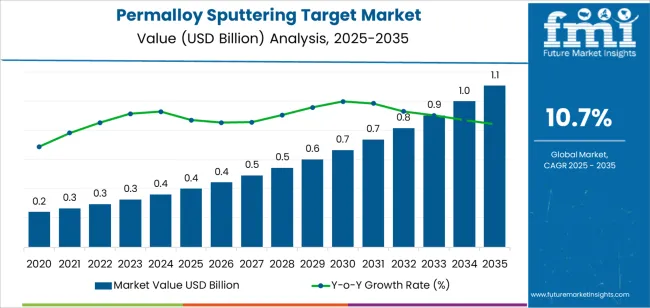
The permalloy sputtering target market is projected to expand from USD 0.4 billion in 2025 to USD 1.1 billion by 2035, recording an absolute increase of USD 0.7 billion and rising at a CAGR of 10.7%. This nearly 2.8X growth is driven by the surging adoption of magnetic thin film materials in advanced electronics manufacturing and the expanding application base of magnetoresistive sensors across precision instruments, data storage devices, and magnetic shielding systems. The transition toward high-purity permalloy alloys with optimized nickel-iron ratios is reinforcing the role of these sputtering targets in achieving stable magnetic permeability and minimal coercivity during thin film deposition operations. Their deployment across semiconductor fabrication, magnetic sensor production, and data storage coating facilities is becoming a crucial performance differentiator for achieving magnetic consistency and signal integrity.
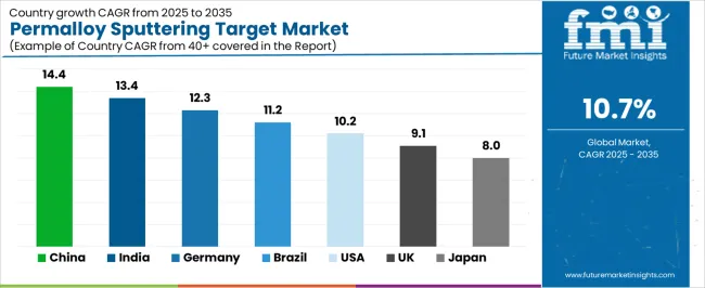
From 2025 to 2030, the market will rise from USD 0.4 billion to USD 0.6 billion, accounting for 28.5% of total value growth. This early phase will emphasize integration of permalloy sputtering materials with automated physical vapor deposition systems, supporting demand from sensor and chip manufacturing ecosystems. Between 2030 and 2035, market growth accelerates, adding USD 0.5 billion, or 71.5% of the decade’s total expansion, reflecting the adoption of customized permalloy compositions for enhanced performance in miniaturized and high-frequency electronics applications. The round target shape dominates with 44.1% share, favored for its uniform erosion profile and compatibility with rotary magnetron systems. Electronics industry applications lead at 44.1% share, driven by magnetic sensor, data storage, and semiconductor component production, followed by energy (28.0%), medical (16.0%), and aerospace (11.9%) segments. Regionally, China (14.4% CAGR) and India (13.4%) spearhead growth through large-scale electronics expansion and policy incentives under initiatives like Made in China 2025 and Make in India. Germany (12.3%) and Brazil (11.2%) exhibit strong advancement in magnetic materials integration across industrial manufacturing, while the USA (10.2%), UK (9.1%), and Japan (8.0%) maintain precision-driven adoption across sensor, semiconductor, and aerospace applications.
The market demonstrates strong momentum across developed and emerging electronics manufacturing economies, where thin film production industries are transitioning from conventional magnetic materials to permalloy alloys that offer superior magnetic performance characteristics and manufacturing consistency. Permalloy sputtering target technology addresses critical production challenges including precise composition control in nickel-iron alloys, uniform magnetic property maintenance across deposited films, and contamination minimization throughout extended deposition runs. The electronics industry shift toward advanced magnetic sensor technologies and high-density data storage creates steady demand for sputtering materials capable of producing magnetic thin films with minimal coercivity and consistent magnetic response across diverse substrate types. Electronics manufacturers are adopting permalloy sputtering targets for critical applications where magnetic film quality directly impacts device performance and functional reliability requirements. The technology capability to produce soft magnetic films with excellent permeability characteristics reduces device noise and accelerates signal processing capabilities.
Electronics manufacturing facilities and thin film deposition operations are investing in permalloy sputtering target systems to enhance production capabilities through improved magnetic film quality and expanded material processing options. The integration of high-purity alloy compositions and optimized target geometries enables these materials to achieve deposition performance levels exceeding conventional magnetic targets while maintaining compositional accuracy standards. The initial material cost considerations for specialized alloy targets and technical expertise requirements for optimal deposition parameter selection may pose challenges to market expansion in cost-sensitive manufacturing segments and regions with limited access to thin film processing expertise and material characterization resources.
Between 2025 and 2030, the permalloy sputtering target market is projected to expand from USD 0.4 billion to USD 0.6 billion, resulting in a value increase of USD 0.2 billion, which represents 28.5% of the total forecast growth for the decade. This phase of development will be shaped by rising demand for magnetic thin film materials in electronics production, product innovation in alloy composition technology and target manufacturing processes, as well as expanding integration with advanced sputtering equipment and automated deposition systems. Companies are establishing competitive positions through investment in high-purity material processing, optimized target geometries, and strategic market expansion across semiconductor manufacturing facilities, magnetic sensor production operations, and specialized thin film coating services.
From 2030 to 2035, the market is forecast to grow from USD 0.6 billion to USD 1.1 billion, adding another USD 0.5 billion, which constitutes 71.5% of the overall ten-year expansion. This period is expected to be characterized by the expansion of specialized permalloy formulations, including customized composition ratios and enhanced purity grades tailored for specific deposition requirements and application demands, strategic collaborations between target material manufacturers and equipment suppliers, and an enhanced focus on deposition efficiency optimization and film quality enhancement. The growing focus on magnetic sensor precision and data storage density will drive demand for advanced, high-performance permalloy sputtering target solutions across diverse electronics manufacturing applications.
| Metric | Value |
|---|---|
| Market Value (2025) | USD 0.4 billion |
| Market Forecast Value (2035) | USD 1.1 billion |
| Forecast CAGR (2025-2035) | 10.7% |
The permalloy sputtering target market grows by enabling manufacturers to achieve superior magnetic thin film quality and deposition consistency while meeting precise compositional requirements in advanced electronics production. Manufacturing facilities face mounting pressure to improve magnetic film performance and production reliability, with permalloy sputtering targets typically providing excellent soft magnetic properties and superior compositional control compared to alternative magnetic materials, making these specialized targets essential for competitive electronics manufacturing operations. The magnetic sensor and data storage industries need for precise magnetic film deposition creates demand for advanced sputtering materials that can maintain tight compositional tolerances, achieve consistent magnetic characteristics, and ensure reliable film quality across diverse production volumes and substrate configurations.
Electronics manufacturing initiatives promoting thin film technology and precision deposition drive adoption in semiconductor facilities, magnetic sensor production operations, and specialty coating services, where magnetic film quality has a direct impact on device performance and manufacturing yields. The global shift toward advanced sensor technologies and high-density storage implementation accelerates permalloy sputtering target demand as electronics facilities seek deposition materials that optimize magnetic properties and maximize production consistency. Limited awareness of optimal alloy composition selection and higher material costs compared to standard magnetic targets may limit adoption rates among smaller electronics manufacturers and regions with traditional thin film practices and limited access to material science expertise and deposition optimization support.
The market is segmented by target shape, application, and region. By target shape, the market is divided into round target, rectangular target, and special shaped target. Based on application, the market is categorized into electronics industry, energy field, medical field, and aerospace. Regionally, the market is divided into Asia Pacific, Europe, North America, Latin America, and Middle East & Africa.

The round target segment represents the dominant force in the market, capturing approximately 44.1% of total market share in 2025. This category encompasses circular target configurations optimized for rotary magnetron sputtering systems, delivering uniform erosion patterns and efficient material utilization across diverse deposition applications. The round target segment market leadership stems from its widespread equipment compatibility, established production infrastructure, and cost-effective manufacturing characteristics across semiconductor fabrication and magnetic sensor production facilities.
The rectangular target segment maintains a substantial 36.0% market share, serving manufacturers who require planar magnetron configurations through linear target geometries and specialized deposition patterns suited for large-area coating applications and batch processing systems. The special shaped target segment represents 19.9% market share through customized applications requiring unique target geometries and application-specific configurations for specialized deposition equipment and research development programs.
Key advantages driving the round target segment include:

Electronics industry applications dominate the market with approximately 44.1% market share in 2025, reflecting the extensive utilization of magnetic thin film materials across magnetic sensor manufacturing, data storage component production, and semiconductor device fabrication. The electronics industry segment market leadership is reinforced by widespread implementation in magnetoresistive sensor production, magnetic read head fabrication, and magnetic shielding applications, which provide essential magnetic performance advantages and device functionality in high-volume electronics manufacturing environments.
The energy field segment represents 28.0% market share through specialized applications including magnetic components for power systems, energy harvesting devices, and electromagnetic shielding solutions requiring soft magnetic film properties. Medical field accounts for 16.0% market share, driven by adoption in medical sensor devices, diagnostic equipment components, and biomedical instrumentation where magnetic sensing capabilities support clinical measurement requirements. Aerospace represents 11.9% market share through applications in navigation systems, aerospace sensors, and specialized magnetic shielding where reliability and performance consistency are critical.
Key market dynamics supporting application preferences include:
The market is driven by three concrete demand factors tied to electronics performance and manufacturing quality. First, magnetic sensor technology expansion creates increasing requirements for soft magnetic thin films, with global electronics manufacturers implementing advanced magnetoresistive sensors requiring reliable permalloy sputtering targets for magnetic film deposition, sensor element fabrication, and device performance optimization. Second, data storage industry advancement and recording density improvement drive adoption of precision magnetic materials, with permalloy sputtering targets improving magnetic film quality while enabling higher storage densities in hard disk drive production and magnetic recording applications. Third, electronics miniaturization initiatives and sensor integration requirements accelerate deployment across manufacturing facilities, with permalloy sputtering targets integrating effectively into thin film deposition processes and enabling precise magnetic property control in miniaturized electronic devices.
Market restraints include material cost barriers affecting manufacturers in price-sensitive market segments and budget-constrained production operations, particularly where alternative magnetic materials remain adequate for less demanding applications and where material budgets constrain adoption of specialized permalloy alloy targets. Technical parameter optimization requirements for deposition process control pose adoption challenges for facilities lacking thin film expertise, as permalloy sputtering effectiveness depends heavily on proper power settings, pressure optimization, and substrate temperature control that vary significantly across equipment configurations and application requirements. Limited availability of material characterization capabilities in emerging electronics manufacturing markets creates additional barriers, as production facilities require analytical equipment for composition verification, magnetic property testing, and film quality assessment to achieve target deposition specifications.
Key trends indicate accelerated adoption in Asian electronics manufacturing hubs, particularly China and India, where semiconductor fabrication and electronics component production are expanding rapidly through government industrialization programs and foreign investment in electronics manufacturing infrastructure. Technology advancement trends toward ultra-high purity permalloy compositions with enhanced magnetic softness, nanocrystalline target structures for improved film properties, and bonded target assemblies enabling optimized thermal management are driving next-generation material development. The market thesis could face disruption if alternative magnetic materials including amorphous alloys achieve breakthrough capabilities in soft magnetic performance, potentially reducing demand for conventional permalloy targets in specific application segments.
| Country | CAGR (2025 to 2035) |
|---|---|
| China | 14.4% |
| India | 13.4% |
| Germany | 12.3% |
| Brazil | 11.2% |
| USA | 10.2% |
| UK | 9.1% |
| Japan | 8.0% |
The market is gaining momentum worldwide, with China taking the leads to aggressive electronics manufacturing expansion and semiconductor industry development programs. Close behind, India benefits from growing electronics production capabilities and government manufacturing initiatives, positioning itself as a strategic growth hub in the Asia-Pacific region. Brazil shows strong advancement, where expanding electronics manufacturing and industrial capability development strengthen its role in South American thin film materials markets. The USA demonstrates robust growth through advanced sensor technology development and data storage innovation, signaling continued adoption in precision magnetic film applications. Meanwhile, Japan stands out for its thin film technology expertise and magnetic materials engineering integration, while UK and Germany continue to record consistent progress driven by electronics manufacturing facilities and sensor technology development centers. Together, China and India anchor the global expansion story, while established markets build stability and technological leadership into the market growth path.
The report covers an in-depth analysis of 40+ countries, top-performing countries are highlighted below.

China demonstrates the strongest growth potential in the market with a CAGR of 14.4% through 2035. The country leadership position stems from comprehensive electronics manufacturing expansion, intensive semiconductor industry development programs, and aggressive thin film materials market growth targets driving adoption of specialized sputtering technologies. Growth is concentrated in major electronics manufacturing regions, including Jiangsu, Guangdong, Shanghai, and Zhejiang, where semiconductor fabrication facilities, magnetic sensor manufacturers, and thin film coating operations are implementing permalloy sputtering target systems for production quality enhancement and manufacturing capability improvement. Distribution channels through materials distributors, sputtering equipment suppliers, and direct manufacturer relationships expand deployment across electronics clusters, semiconductor production bases, and thin film manufacturing centers. The country Made in China 2025 initiative provides policy support for advanced materials technology adoption, including incentives for specialty material implementation and manufacturing upgrading programs.
Key market factors:
In major electronics manufacturing regions including Karnataka, Maharashtra, Tamil Nadu, and Gujarat industrial zones, the adoption of permalloy sputtering targets is accelerating across semiconductor facilities, electronics manufacturing operations, and thin film coating services, driven by Make in India initiatives and increasing focus on electronics manufacturing competitiveness. The market demonstrates strong growth momentum with a CAGR of 13.4% through 2035, linked to comprehensive electronics sector expansion and increasing investment in thin film deposition capabilities. Indian manufacturers are implementing permalloy sputtering target technology and advanced deposition systems to improve production quality while meeting stringent performance requirements in electronics manufacturing operations serving domestic and export markets. The country electronics manufacturing policies create steady demand for advanced sputtering materials, while increasing focus on production quality drives adoption of specialized magnetic thin film materials that enhance manufacturing competitiveness.
Germany advanced electronics sector demonstrates sophisticated implementation of permalloy sputtering targets, with documented production studies showing significant quality improvements in magnetic film deposition through optimized materials strategies. The country manufacturing infrastructure in major industrial regions, including Bavaria, Baden-Wurttemberg, North Rhine-Westphalia, and Saxony, showcases integration of specialized sputtering materials with existing thin film capabilities, leveraging expertise in precision manufacturing and materials engineering. German manufacturers emphasize quality standards and process optimization, creating demand for reliable sputtering materials that support production commitments and stringent magnetic property requirements. The market maintains strong growth through focus on Industry 4.0 integration and manufacturing excellence, with a CAGR of 12.3% through 2035.
Key development areas:
The Brazilian market leads in Latin American permalloy sputtering target adoption based on expanding electronics manufacturing operations and growing thin film capability in major industrial centers. The country shows solid potential with a CAGR of 11.2% through 2035, driven by electronics sector investment and increasing demand for specialized materials across electronics production, sensor manufacturing, and industrial coating sectors. Brazilian manufacturers are adopting permalloy sputtering target technology for compliance with international quality standards, particularly in electronics manufacturing requiring precise magnetic films and in sensor production where material quality impacts device performance. Technology deployment channels through materials distributors, equipment suppliers, and procurement programs expand coverage across electronics supply chains and manufacturing facilities.
Leading market segments:
The USA market leads in advanced permalloy sputtering target applications based on integration with sophisticated magnetic sensor systems and comprehensive data storage technologies for enhanced device performance. The country shows solid potential with a CAGR of 10.2% through 2035, driven by sensor technology leadership and increasing adoption of advanced magnetic materials across electronics manufacturing, defense applications, and aerospace sensor systems. American manufacturers are implementing permalloy sputtering targets for high-precision deposition requirements, particularly in magnetoresistive sensor production demanding precise magnetic properties and in data storage manufacturing where film quality directly impacts storage density and device reliability. Technology deployment channels through specialty materials distributors, equipment suppliers, and direct manufacturer relationships expand coverage across diverse electronics operations.
Leading market segments:
The UK market demonstrates consistent implementation focused on electronics manufacturing and sensor technology development, with documented materials integration achieving quality improvements in thin film deposition operations. The country maintains steady growth momentum with a CAGR of 9.1% through 2035, driven by electronics manufacturing presence and magnetic materials requirements in advanced device applications. Major industrial regions, including South East England, West Midlands, and Scotland, showcase deployment of specialized sputtering materials that integrate with existing manufacturing infrastructure and support quality requirements in electronics production chains.
Key market characteristics:
Japan permalloy sputtering target market demonstrates sophisticated implementation focused on electronics manufacturing excellence and magnetic materials engineering, with documented integration of specialized sputtering materials achieving quality advancements in precision thin film deposition operations. The country maintains steady growth momentum with a CAGR of 8.0% through 2035, driven by manufacturing excellence culture and focus on materials quality principles aligned with precision manufacturing standards. Major industrial regions, including Tokyo, Osaka, Aichi, and Kyushu, showcase advanced deployment of specialized sputtering materials that integrate seamlessly with thin film production lines and comprehensive quality control systems.
Key market characteristics:
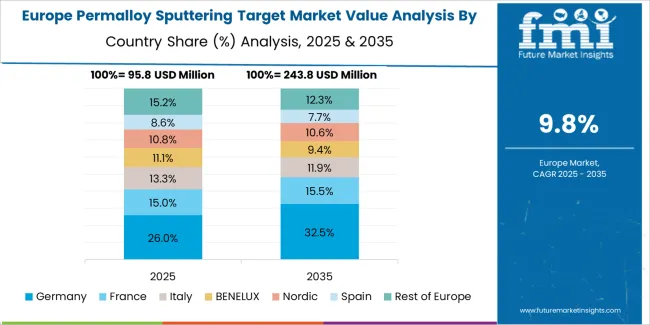
The permalloy sputtering target market in Europe is projected to grow from USD 107.9 million in 2025 to USD 328.0 million by 2035, registering a CAGR of 11.8% over the forecast period. Germany is expected to maintain its leadership position with a 31.2% market share in 2025, declining slightly to 30.5% by 2035, supported by its extensive electronics manufacturing infrastructure and major industrial centers, including Bavaria, Baden-Wurttemberg, and North Rhine-Westphalia production regions.
France follows with a 23.6% share in 2025, projected to reach 24.0% by 2035, driven by comprehensive electronics component production and thin film technology programs in major industrial regions. The United Kingdom holds a 19.8% share in 2025, expected to reach 20.1% by 2035 through electronics manufacturing facilities and sensor technology operations. Italy commands a 13.4% share in both 2025 and 2035, backed by electronics production and precision manufacturing. Spain accounts for 6.2% in 2025, rising to 6.4% by 2035 on electronics manufacturing expansion and technology sector growth. The Rest of Europe region is anticipated to hold 5.8% in 2025, expanding to 6.6% by 2035, attributed to increasing permalloy sputtering target adoption in Nordic countries and emerging Central & Eastern European electronics manufacturing operations.

The Japanese permalloy sputtering target market demonstrates a mature and quality-focused landscape, characterized by sophisticated integration of specialized magnetic materials with existing thin film deposition infrastructure across electronics manufacturing facilities, magnetic sensor production operations, and precision coating services. Japan focus on manufacturing excellence and materials quality drives demand for high-purity sputtering targets that support production commitments and magnetic property targets in competitive electronics environments. The market benefits from strong partnerships between international materials providers and domestic electronics distributors including major trading companies, creating comprehensive service ecosystems that prioritize technical support and application engineering programs. Manufacturing centers in Tokyo, Osaka, Aichi, and other major industrial areas showcase advanced thin film implementations where permalloy sputtering targets achieve high deposition quality through optimized materials specifications and comprehensive process control systems.

The South Korean permalloy sputtering target market is characterized by growing international materials provider presence, with companies maintaining significant positions through comprehensive technical support and application engineering capabilities for electronics manufacturing operations and thin film deposition applications. The market demonstrates increasing focus on manufacturing quality and materials innovation, as Korean manufacturers increasingly demand specialized sputtering materials that integrate with domestic production infrastructure and sophisticated manufacturing management systems deployed across major industrial complexes. Regional materials distributors are gaining market share through strategic partnerships with international manufacturers, offering specialized services including technical training programs and application-specific materials solutions for electronics and sensor production operations. The competitive landscape shows increasing collaboration between multinational materials companies and Korean industrial specialists, creating hybrid service models that combine international product development expertise with local technical support capabilities and rapid response systems.
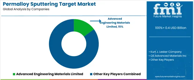
The market features approximately 15-20 meaningful players with moderate fragmentation, where leading companies control market share through established distribution networks and comprehensive product portfolios. Competition centers on material purity consistency, compositional accuracy, and technical support capabilities rather than price competition alone. Market leaders maintain competitive advantages through specialized metallurgical expertise and established relationships with electronics manufacturers and thin film deposition facilities.
Market leaders include specialized materials manufacturers with focused expertise and comprehensive sputtering target capabilities, which maintain competitive advantages through metallurgical knowledge, quality control systems, and deep application understanding across multiple electronics sectors, creating trust and reliability advantages with semiconductor fabrication operations and magnetic sensor manufacturing facilities. These companies leverage research and development capabilities in alloy composition optimization, purity enhancement technology, and ongoing technical support relationships to defend market positions while expanding into emerging electronics markets and specialized application segments.
Challengers encompass regional materials suppliers and thin film materials specialists, which compete through differentiated product offerings and strong regional presence in key electronics manufacturing markets. Product specialists focus on specific target configurations or purity grades, offering specialized capabilities in custom composition solutions, rapid delivery services, and competitive pricing structures for standard target specifications.
Regional players and emerging materials manufacturers create competitive pressure through localized production advantages and application responsiveness capabilities, particularly in high-growth markets including China and India, where proximity to electronics manufacturing clusters provides advantages in technical support responsiveness and customer relationships. Market dynamics favor companies that combine proven materials performance with comprehensive technical support offerings that address the complete deposition cycle from target bonding through process optimization and film characterization.
Permalloy sputtering targets represent specialized magnetic materials that enable manufacturers to achieve precise magnetic thin film deposition and superior soft magnetic properties while improving device performance, delivering excellent compositional control and deposition consistency with enhanced magnetic characteristics and manufacturing reliability in demanding electronics applications. With the market projected to grow from USD 0.4 billion in 2025 to USD 1.1 billion by 2035 at a 10.7% CAGR, these specialized sputtering materials offer compelling advantages - magnetic property optimization, deposition precision, and film quality - making them essential for electronics industry applications (44.1% market share), energy field operations (28.0% share), and manufacturing facilities seeking alternatives to conventional magnetic materials that compromise performance through inconsistent magnetic properties and inferior compositional control. Scaling market adoption and technology deployment requires coordinated action across materials policy, manufacturing infrastructure development, materials manufacturers, electronics facilities, and industrial materials investment capital.
| Item | Value |
|---|---|
| Quantitative Units | USD 0.4 billion |
| Target Shape | Round Target, Rectangular Target, Special Shaped Target |
| Application | Electronics Industry, Energy Field, Medical Field, Aerospace |
| Regions Covered | Asia Pacific, Europe, North America, Latin America, Middle East & Africa |
| Country Covered | China, India, Germany, Brazil, USA, UK, Japan, and 40+ countries |
| Key Companies Profiled | Advanced Engineering Materials Limited, Kurt J. Lesker Company, QS Advanced Materials Inc, Nanografi, Zhengzhou Tainuo Film Materials Co., Ltd., Zhengzhou CY Scientific Instrument Co., Ltd., RD Mathis Company, Proterial (India) Private Limited |
| Additional Attributes | Dollar sales by target shape and application categories, regional adoption trends across Asia Pacific, Europe, and North America, competitive landscape with materials manufacturers and distribution networks, manufacturing facility requirements and technical specifications, integration with sputtering equipment and thin film deposition systems, innovations in alloy composition technology and purity enhancement platforms, and development of specialized magnetic materials with enhanced deposition performance and film quality capabilities. |
The global permalloy sputtering target market is estimated to be valued at USD 0.4 billion in 2025.
The market size for the permalloy sputtering target market is projected to reach USD 1.1 billion by 2035.
The permalloy sputtering target market is expected to grow at a 10.7% CAGR between 2025 and 2035.
The key product types in permalloy sputtering target market are round target, rectangular target and special shaped target.
In terms of application, electronics industry segment to command 44.1% share in the permalloy sputtering target market in 2025.






Full Research Suite comprises of:
Market outlook & trends analysis
Interviews & case studies
Strategic recommendations
Vendor profiles & capabilities analysis
5-year forecasts
8 regions and 60+ country-level data splits
Market segment data splits
12 months of continuous data updates
DELIVERED AS:
PDF EXCEL ONLINE
Sputtering Targets Market Growth - Trends & Forecast 2025 to 2035
Zinc-tin Alloy Sputtering Target Market Size and Share Forecast Outlook 2025 to 2035
Demand for Zinc-Tin Alloy Sputtering Target in UK Size and Share Forecast Outlook 2025 to 2035
Target-based ADME/ Tox Assay Market
Targeting Pods Market
RNA-Targeted Small Molecules Market – Trends & Forecast 2024-2034
Rosacea-Targeting Skincare Market Analysis - Size and Share Forecast Outlook 2025 to 2035
Complement-targeted Therapeutics Market
NRG1 Fusion-Targeted Therapy Market Analysis - Size, Share, and Forecast Outlook 2025 to 2035
Molybdenum-niobium Alloy Target Market Size and Share Forecast Outlook 2025 to 2035
Demand for Molybdenum-niobium Alloy Target in UK Size and Share Forecast Outlook 2025 to 2035
Demand for Molybdenum-niobium Alloy Target in USA Size and Share Forecast Outlook 2025 to 2035

Thank you!
You will receive an email from our Business Development Manager. Please be sure to check your SPAM/JUNK folder too.
Chat With
MaRIA