- Market Size (2026)
- USD 1.5 Bn
- Forecast (2036)
- USD 5.2 Bn
- CAGR (2026 to 2036)
- 13.3%
How big is Transition Metal Dichalcogenides Market in 2026?
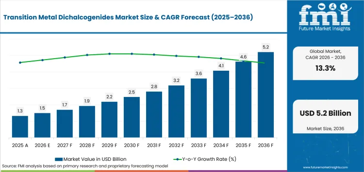
USD 1.5 billion in 2026 and USD 5.2 billion by 2036 at a 13.3% CAGR.
Demand for transition metal dichalcogenides is projected to expand at 13.3% CAGR between 2026 and 2036, increasing valuation from USD 1.5 billion in 2026 to USD 5.2 billion by 2036. Growth is driven by the fact that device teams evaluate these materials alongside semiconductor fabrication materials during qualification of atomically thin electronic channels.
Wafer transfer must preserve a continuous film so contact and dielectric work produce meaningful device comparisons. In January 2025, imec reported more than 99.5% morphological yield from a repeatable 300 mm MX₂ dry-transfer process. The coverage benchmark helps nanomaterials providers document transfer performance, although electrical contacts and gate stacks remain separate qualification gates.
Key Takeaways of Transition Metal Dichalcogenides Market
- Semiconductor scaling programs increase evaluation of atomically thin channels that retain gate control at reduced device dimensions.
- Molybdenum disulfide is projected to account for 34.0% share in 2026 owing to availability across bulk crystals and deposited films.
- Bulk materials are estimated to represent 30.0% share in 2026 due to their upstream role in exfoliation and formulation workflows.
- Nanoelectronics and semiconductors are forecast to capture 33.0% share in 2026 through transistor or memory development programs.
- Optical measurements cannot establish electrical yield across successive material lots, so wafer nonuniformity and interface contamination restrain adoption.
- 2D Semiconductors, ACS Material, Graphenea, Merck, American Elements, HQ Graphene, MSE Supplies and Ossila serve material or integration requirements.
Analyst Perspective
"Commercial TMD qualification depends on reproducing layer thickness and contact behavior across an entire wafer. Device engineers should compare wafer maps with finished transistor yield, since Raman data cannot reveal transfer or gate-stack losses."
- Nikhil Kaitwade, Principal Analyst, Chemicals & Materials, Future Market Insights
How is the Transition Metal Dichalcogenides Market segmented?
The transition metal dichalcogenides industry is segmented by product type, layer type, application, end use, distribution channel and region.
The market is segmented by product type, layer type, application, end use, distribution channel and region. Product type covers molybdenum and tungsten sulfides or selenides, while layer type includes bulk materials, few-layer structures, monolayers and heterostructures. Applications include nanoelectronics, energy systems, optoelectronics and catalysis, while end uses span semiconductor, energy, automotive and aerospace programs. Direct sales and distribution channels reflect requirements for customization, technical support and recurring order scale.
What supports demand for molybdenum disulfide within the product type category?
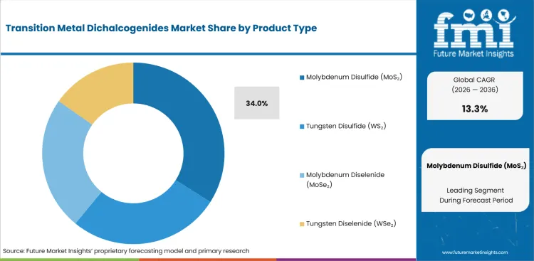
Molybdenum disulfide supports source-crystal studies and deposited-film experiments, allowing laboratories to compare thickness effects without changing the underlying compound. Its long research history provides familiar Raman and electrical benchmarks for repeatable substrate or contact studies.
- Molybdenum disulfide is set to lead the product type with 34.0% share in 2026 due to broad availability across bulk crystals and deposited films.
- Device laboratories use MoS₂ to compare transfer methods and metal contacts across repeated transistor structures. Bulk programs prioritize purity or crystal dimensions, whereas monolayer orders require uniform coverage and documented transfer conditions for commercial material approval.
What role do bulk materials play within the layer type category?
Bulk crystals and powders provide source material for exfoliated flakes or processed derivatives, allowing research teams to verify composition and purity without committing limited early-stage budgets to wafer processing equipment or custom transfer work.
- In 2026, bulk materials are expected to lead layer type with 30.0% share because crystals and powders support exfoliation or formulation work.
- Crystal producers differentiate through purity and lateral dimensions that affect flake size during mechanical exfoliation. Powder programs depend on controlled particle size and lot consistency, which supports repeated catalytic or advanced commercial formulation studies without premature wafer spending commitments.
How does nanoelectronics shape demand within the application category?
Nanoelectronics programs test whether atomically thin channels can retain gate control at dimensions that strain conventional semiconductors. Researchers compare TMD channels with compound semiconductor materials during contact and dielectric studies for logic or memory device test structures.
- Based on application, nanoelectronics and semiconductors are projected to account for 33.0% share in 2026 due to sustained transistor and memory research.
- Device developers need low-resistance contacts and stable threshold behavior across several device structures or thermal cycles. Film producers secure recurring programs by supplying wafer maps and integration records that reduce repeated fabrication experiments during material qualification.
How do direct sales influence selection within the distribution channel category?
Direct orders let laboratories define substrate type, wafer diameter and layer count during film-growth or transfer planning. Custom specifications pair each wafer with semiconductor defect inspection records and electrical maps during incoming material qualification for repeat laboratory orders.
- The direct sales segment is likely to capture 45.0% share in 2026 attributable to custom wafer specifications and application-level coordination for device programs.
- Distributors can handle standard powders or crystals with limited configuration, but monolayer films require direct discussion of coverage and characterization to prevent specification gaps during recurring orders across international research laboratory and device programs.
What are the drivers, restraints and opportunities in the Transition Metal Dichalcogenides Market?
Driver: Atomically thin channels support device scaling. Restraint: Grain boundaries and unstable contacts delay electrical qualification. Opportunity: Wafer maps reduce repeated integration trials.
- Driver: Atomically thin channels improve gate control at dimensions that challenge conventional semiconductor structures in advanced logic programs.
- Restraint: Grain boundaries and transfer residue can change electrical behavior across a wafer despite acceptable optical measurements.
- Opportunity: Wafer maps and process records reduce repeated integration trials during material qualification and device acceptance.
Logic researchers compare TMD channels with graphene-based materials to test gate control at reduced dimensions. Process engineers use semiconductor manufacturing equipment to verify film survival through transfer and gate-stack processing.
Grain boundaries or transfer residue can change current flow across a complete wafer during device testing. Contact resistance and dielectric damage can obscure intrinsic film quality, forcing another fabrication cycle to secure material acceptance.
Energy researchers evaluate TMD electrodes within supercapacitor platforms through cycling tests and controlled surface chemistry. Optical teams assess TMD emitters within photonics platforms through clean interfaces and repeatable spectral measurements.
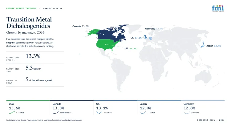
Which country CAGRs are profiled in the Transition Metal Dichalcogenides Market?
| Country | CAGR |
|---|---|
| South Korea | 14.2% |
| United States | 13.6% |
| Canada | 13.3% |
| United Kingdom | 13.1% |
| Australia | 13.0% |
| Japan | 12.9% |
| Germany | 12.8% |
How do country-level CAGRs compare in the Transition Metal Dichalcogenides Market?
The country forecasts are tightly grouped across the transition metal dichalcogenides (TMDs) market, with only 1.4 percentage points separating South Korea and Germany. South Korea and the United States form a small upper group, while Canada, the UK, Australia, Japan and Germany remain clustered within a narrow range. The limited spread suggests that TMD research and commercialization are progressing across multiple advanced materials ecosystems at a comparable pace. Growth is largely tied to semiconductor innovation, nanomaterials research and emerging applications in electronics, photonics and sensing technologies.
- South Korea benefits from strong semiconductor and display manufacturing capabilities.
- The United States supports growth through extensive nanotechnology research and commercialization efforts.
- Canada reflects increasing investment in advanced materials and academic-industry collaboration.
- The United Kingdom continues to expand through research focused on next-generation electronic materials.
- Australia benefits from growing activity in materials science and advanced manufacturing.
- Japan maintains demand through its established electronic materials industry.
- Germany supports adoption through strong industrial R&D and semiconductor innovation initiatives.
Comparable CAGRs may still reflect different market conditions because research funding, commercialization pathways and semiconductor ecosystems vary across countries. The full report provides country-level CAGR analysis across North America, Latin America, Europe, East Asia, South Asia, Oceania and the Middle East and Africa.
Country-wise Analysis
- South Korea’s memory-fabrication ecosystem gives materials laboratories access to pilot lines that compare atomically thin channels with established deposition and device processes for transistor or advanced-packaging programs during commercial material screening and device qualification. In March 2026, MOTIR increased its international industrial technology cooperation budget by 11% and outlined long-term overseas research hubs with defined milestones for next-generation manufacturing technologies supporting durable international engineering partnerships for manufacturers. Transition metal dichalcogenide sales in South Korea are forecast to expand at 14.2% CAGR by 2036, supported by dense engineering networks despite demanding local service and detailed process-documentation requirements for overseas film producers.
- United States semiconductor programs combine national metrology resources with commercial nanofabrication facilities that support material screening and reliability studies through repeated qualification cycles for distinct transistor designs and investment decisions within domestic research programs. Adoption of transition metal dichalcogenides in the United States is estimated to expand at 13.6% CAGR through 2036, reinforced by repeatable measurement capability despite unresolved contact and lifetime testing across commercial device platforms. In March 2025, NIST updated its 2D-material reliability project to develop electrical and mechanical stress methods with lifetime analyses for large-scale manufacturing that direct film qualification toward transferability between fabrication tools during trials.
- Canada’s shared nanotechnology facilities give university teams and device developers access to materials analysis and integrated-photonics testing without maintaining complete fabrication infrastructure at every research site during early commercial material and device qualification work. In August 2025, the National Research Council described advanced-materials laboratories and integrated-photonics capabilities that support prototype development and device testing across collaborative electronic or photonic programs for device teams seeking repeatable access nationwide. Canada's transition metal dichalcogenides outlook is anticipated to advance at 13.3% CAGR over the assessment period, aided by shared facilities despite limited domestic wafer-scale growth and specialized transfer capacity for recurring commercial programs.
- United Kingdom semiconductor developers can use university cleanrooms and specialist facilities, yet TMD programs must bridge the gap between research samples and repeat manufacturing evidence for several wafer lots and commercial device designs. Transition metal dichalcogenide demand in the United Kingdom is forecast to rise at 13.1% CAGR over the forecast period, driven by commercialization support despite limited domestic volume fabrication and demanding wafer-reliability evidence requirements. In September 2025, the government launched a semiconductor commercialization fund that gives eligible companies access to ultra-clean facilities and technical expertise during product development or early manufacturing preparation for commercial trials within semiconductor programs.
- Australia’s TMD activity remains concentrated in university laboratories, so specialized films and replacement materials travel long distances between research centers and device-development sites with limited domestic transfer capacity or rapid replacement inventory for trials. In January 2025, a Monash study demonstrated large-scale electrode-array transfer with eight elemental metals on monolayer TMD semiconductors and gave local teams a practical contact-engineering route for device experiments that require repeat material deliveries. By 2036, Australia is projected to grow at 13.0% CAGR, influenced by photonics and commercial device research despite limited local wafer-transfer services and long delivery routes between specialized laboratories across the country.
- Japan’s semiconductor ecosystem supports detailed materials characterization and controlled process transfer across universities and national laboratories that evaluate unfamiliar atomically thin channels for advanced electronic programs during repeated pilot fabrication and commercial material approval. In April 2025, NIMS established a dedicated 2D Semiconductor Group focused on high-quality materials and device fabrication processes that directly connect TMD research with practical integration evidence for next-generation electronic programs and commercial translation. Japan is estimated to post 12.9% CAGR over the forecast period, reinforced by deep local device expertise despite long acceptance cycles and repeated proof requirements across separate integration conditions and wafer lots.
- Germany links applied materials laboratories with photonics and microelectronics clusters that can take TMD concepts from synthesis into device evaluation and commercial pilot manufacturing across regional research centers and specialized semiconductor development facilities. The University of Jena presented its 2DMat-Lith-Lab project in May 2025 for electronic or optoelectronic devices based on graphene and TMDs within regional research programs that connect material synthesis with lithography and device prototyping. The German transition metal dichalcogenides sector is projected to record 12.8% CAGR during the assessment period, shaped by device research despite fragmented pilot volumes and demanding commercial material qualification across specialized process conditions.
Who are the notable companies in the Transition Metal Dichalcogenides Market?
2D Semiconductors Inc., ACS Material LLC, Graphenea S.A., Merck KGaA, American Elements, HQ Graphene, MSE Supplies LLC and Ossila Ltd. are the notable companies serving this market.
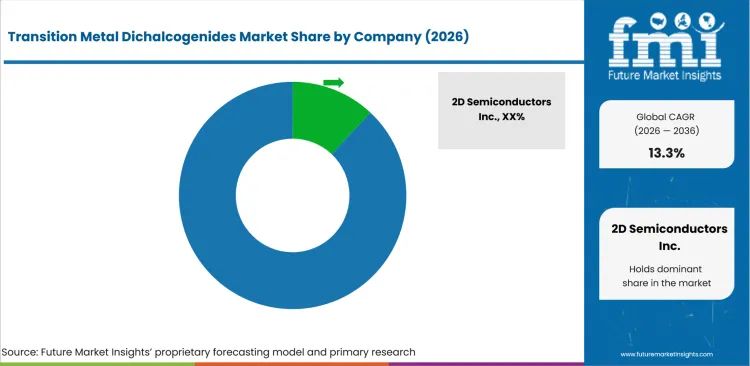
The market remains fragmented as laboratories purchase small lots with compound-specific purity and substrate requirements. Wafer-scale entry requires consistent coverage and electrical behavior across repeated material lots during device qualification.
- 2D Semiconductors, HQ Graphene and Ossila focus on TMD coverage across crystals, powders and films.
- ACS Material, Merck, American Elements and MSE Supplies extend access through catalogs and international distribution.
- Graphenea connects TMD handling with wafer transfer and silicon-platform integration for optoelectronic or semiconductor development.
Competitive Benchmarking: Transition Metal Dichalcogenides Market
| Company | TMD product breadth | Layer and form coverage | Custom growth or integration support | Geographic Reach |
|---|---|---|---|---|
| 2D Semiconductors Inc. | High | High | High | International research market |
| ACS Material LLC | High | High | Low | United States and international supply |
| Graphenea S.A. | Low | Low | High | Europe and United States |
| Merck KGaA | High | High | Medium | Global |
| American Elements | High | High | Medium | Global |
| HQ Graphene | High | Low | Medium | Europe and international research market |
| MSE Supplies LLC | High | High | Low | United States and international supply |
| Ossila Ltd. | High | High | Low | United Kingdom and international supply |
Key Developments in the Transition Metal Dichalcogenides Market
- In July 2025, AIXTRON SE received a Cambridge order for a 200 mm deposition system supporting wafer-scale layered-material growth in photonics research.
- In June 2026, AIXTRON SE announced two Hyperion systems for MIT Lincoln Laboratory supporting two-dimensional materials research across 200 mm and 300 mm processing.
- In June 2026, imec and ASML-TSMC partners demonstrated 300 mm transistors using MoS₂, WS₂ and WSe₂ with 94% operational devices.
Key Players in the Transition Metal Dichalcogenides Market
Specialist TMD film and crystal producers
- 2D Semiconductors Inc.
- HQ Graphene
- Ossila Ltd.
Broad advanced-materials suppliers
- ACS Material LLC
- Merck KGaA
- American Elements
- MSE Supplies LLC
Wafer-integration platforms
- Graphenea S.A.
Transition Metal Dichalcogenides Market - Report Scope
| Coverage field | Report scope |
|---|---|
| Market breakdown | By product type, layer type, application, end use, distribution channel and region. |
| Quantitative Units | Revenue in USD Billion and CAGR in % |
| Market Definition | Commercial TMD crystals, powders, films, wafers and heterostructures used across approved applications. |
| Regions Covered | North America, Latin America, Europe, East Asia, South Asia, Oceania and Middle East and Africa |
| Countries Covered | South Korea, United States, Canada, United Kingdom, Australia, Japan and Germany. |
| Key Companies Profiled | 2D Semiconductors Inc., ACS Material LLC, Graphenea S.A., Merck KGaA, American Elements, HQ Graphene, MSE Supplies LLC and Ossila Ltd. |
| Forecast Period | 2026 to 2036. |
| Approach | Primary and secondary research with market triangulation. |
Transition Metal Dichalcogenides Market - Research Methodology
| Method | Approach |
|---|---|
| Primary Research | FMI analysts gathered input from manufacturers, service providers, technology developers, distributors, end users, procurement teams, and subject-matter experts. Interviews examined purchasing decisions, product or service evaluation, adoption barriers, approval requirements, pricing considerations, and expectations for technical or commercial support. Respondents were also asked what evidence is required before a trial, pilot, or initial order develops into regular purchasing. |
| Desk Research | Desk research covered government statistics, regulatory publications, trade data, industry associations, technical literature, standards, company filings, product information, and official corporate announcements. Sources were reviewed for relevance, publication date, geographic coverage, and consistency with the defined market scope. Claims relating to performance, applications, approvals, capacity, investment, and commercial activity were retained only when supported by credible public evidence. |
| Market Sizing and Forecasting | The market model combined the baseline value with historical performance, segment structure, pricing and volume indicators, adoption levels, company participation, and country-level demand conditions. Forecast assumptions considered economic activity, investment trends, regulatory developments, technology adoption, purchasing cycles, supply availability, and barriers to wider market use. Segment and regional estimates were reconciled before the final market total was calculated. |
| Data Validation | Estimates were checked against multiple independent indicators, including public data, company activity, trade patterns, industry developments, and findings from primary interviews. Validation also tested whether products, services, applications, and company revenues fell within the defined market boundaries. Adjacent categories, unsupported claims, overlapping revenues, and activities without direct market relevance were excluded to reduce double counting and maintain consistency across segments and countries. |
Transition Metal Dichalcogenides Market by Segments
Transition Metal Dichalcogenides Market segmented by Product Type:
- Molybdenum Disulfide (MoS₂)
- Monolayer MoS₂
- Bulk MoS₂
- Tungsten Disulfide (WS₂)
- Monolayer WS₂
- Bulk WS₂
- Molybdenum Diselenide (MoSe₂)
- Monolayer MoSe₂
- Bulk MoSe₂
- Tungsten Diselenide (WSe₂)
- Monolayer WSe₂
- Bulk WSe₂
Transition Metal Dichalcogenides Market segmented by Layer Type:
- Bulk
- Bulk Crystals
- Bulk Powders
- Few-Layer
- Bilayer Materials
- Multilayer Materials
- Monolayer
- CVD-Grown Monolayers
- Mechanically Exfoliated Monolayers
- Heterostructures
- Van der Waals Heterostructures
- Stacked 2D Heterostructures
Transition Metal Dichalcogenides Market segmented by Application:
- Nanoelectronics & Semiconductors
- Field-Effect Transistors
- Logic & Memory Devices
- Energy Storage & Conversion
- Battery Electrodes
- Supercapacitors
- Optoelectronics
- Photodetectors
- Light-Emitting Devices
- Catalysis
- Hydrogen Evolution Reaction
- Electrocatalysis
Transition Metal Dichalcogenides Market segmented by End Use:
- Semiconductor & Electronics
- Integrated Device Manufacturers
- Electronic Component Manufacturers
- Energy
- Battery Manufacturers
- Renewable Energy Technology Developers
- Automotive
- Electric Vehicles
- Automotive Sensors
- Aerospace & Defense
- Avionics
- Advanced Sensing Systems
Transition Metal Dichalcogenides Market segmented by Distribution Channel:
- Direct Sales
- Direct Manufacturer Sales
- Custom Material Orders
- Distributors
- Specialty Chemical Distributors
- Advanced Material Distributors
- Online Retailers
- E-Commerce Platforms
- Scientific Supply Websites
- Research & Laboratory Suppliers
- University Procurement
- Research Laboratory Suppliers
Transition Metal Dichalcogenides Market by Region:
- North America
- United States
- Canada
- Latin America
- Brazil
- Chile
- Mexico
- Rest of Latin America
- Western Europe
- Germany
- United Kingdom
- Italy
- Spain
- France
- Nordics
- Benelux
- Rest of Western Europe
- Eastern Europe
- Russia
- Poland
- Hungary
- Balkan and Baltic States
- Rest of Eastern Europe
- East Asia
- China
- Japan
- South Korea
- South Asia and Pacific
- India
- ASEAN
- Australia and New Zealand
- Rest of South Asia and Pacific
- Middle East and Africa
- Kingdom of Saudi Arabia
- Other GCC Countries
- Türkiye
- South Africa
- Other African Union Countries
- Rest of Middle East and Africa
Research Sources and Bibliography
- imec. (2025, January 16). Introducing 2D-material based devices in the logic scaling roadmap.
- Ministry of Trade, Industry and Resources. (2026, March 9). MOTIR Expands Global R&D Program to Support Manufacturing AX and Industrial Innovation.
- National Institute of Standards and Technology. (2025, March 26). Evaluation of 2D and WBG Material Quality Toward Device Reliability.
- National Research Council Canada. (2025, August 6). Quantum and Nanotechnologies Research Centre.
- Department for Science, Innovation and Technology. (2025, September 24). New £10 million fund to support UK businesses to deliver next generation of semiconductors.
- Xing, K., McEwen, D., Yin, Y., Zhao, W., Bake, A., Cortie, D., Liu, J., Vu, T. H. Y., Chen, Y. H., Hone, J., Stacey, A., Edmonds, M. T., Medhekar, N. V., Watanabe, K., Taniguchi, T., Ou, Q., Qi, D. C., & Fuhrer, M. S. (2025, January 28). Pick-and-Place Transfer of Arbitrary-Metal Electrodes for van der Waals Device Fabrication.
- National Institute for Materials Science. (2025, April 1). 2D semiconductor group has been established at NIMS.
- Friedrich Schiller University Jena. (2025, May 12). InnoCON Thüringen 2025.
- imec. (2026, June 15). ASML, TSMC and imec bring industry-ready 2D-material transistors closer with breakthrough 300mm integration.
- AIXTRON SE. (2025, July 15). University of Cambridge chooses AIXTRON tool for next generation 2D/layered materials-based photonic devices.
- AIXTRON SE. (2026, June 23). MIT Lincoln Laboratory invests in two AIXTRON Hyperion 300 mm systems to advance GaN and 2D materials research.
- 2D Semiconductors Inc. (2026). 2-inch wafer CVD monolayers or few-layers. Retrieved August 4, 2026.
- ACS Material LLC. (2026). Graphene-like materials. Retrieved August 4, 2026.
- Graphenea S.A. (2026). Graphenea and the WOW-2D Consortium: Pioneering wafer-scale integration for 2D optoelectronics.
- Merck KGaA. (2026). Chalcogenides. Retrieved August 4, 2026.
- American Elements. (2026). 2D materials. Retrieved August 4, 2026.
- HQ Graphene. (2026). High-quality 2D crystals. Retrieved August 4, 2026.
- MSE Supplies LLC. (2026). Semiconductor wafers and substrates: 2D materials. Retrieved August 4, 2026.
- Ossila Ltd. (2026). Transition metal dichalcogenides. Retrieved August 4, 2026.
This Report Answers
- How large is the transition metal dichalcogenides market in 2026 and 2036?
- Which operating conditions support demand for transition metal dichalcogenide materials?
- Which product type accounts for the approved 2026 share?
- How do layer types influence commercial material selection?
- Which integration conditions shape transition metal dichalcogenide adoption?
- How do profiled country growth rates differ?
Frequently Asked Questions
How big is the transition metal dichalcogenides market in 2026?
In 2026, the transition metal dichalcogenides market is valued at USD 1.52 billion across electronics and advanced-material applications. Controlled thickness and clean interfaces support recurring commercial orders toward USD 5.31 billion by 2036.
What is the CAGR of the transition metal dichalcogenides market from 2026 to 2036?
The transition metal dichalcogenides market is projected to expand at 13.3% CAGR between 2026 and 2036. Wafer uniformity and contact resistance remain central qualification barriers across repeated semiconductor and optical commercial programs.
Which distribution channel is projected lead the transition metal dichalcogenides market?
Direct sales are projected to account for 45.0% market share by distribution channel in 2026. Custom wafers require defined substrates and layer specifications and documented transfer histories that support recurring commercial orders.
How much will the transition metal dichalcogenides market add between 2026 and 2036?
USD 3.79 billion is expected to be added to the transition metal dichalcogenides market between 2026 and 2036. Film producers need repeatable wafer evidence and dependable technical support during recurring commercial qualification programs.
Which companies are active in the transition metal dichalcogenides market?
Eight profiled companies include 2D Semiconductors and ACS Material alongside Graphenea and Merck across specialized material programs. American Elements and HQ Graphene join MSE Supplies and Ossila through crystals, powders, films and research-scale distribution.
Preview the report firsthand - request a free sample
Get SampleGet the brochure for pricing and purchase details.
Get PDFTable of Content
- Key Takeaways
- Market Size and CAGR
- Top Growth Driver
- Fastest Growing Segment
- Leading Region
- Key Companies
- Emerging Opportunities
- Executive Summary
- Global Market Outlook
- Demand-side Trends
- Supply-side Trends
- Technology Roadmap Analysis
- Analysis and Recommendations
- Analyst Perspective (What is happening? Why now? What should investors know?)
- Key Questions Answered
- How large is the market?
- What is the CAGR?
- What are key trends?
- Which region dominates?
- Who are the leaders?
- Market Overview
- Market Coverage / Taxonomy
- Market Definition / Scope / Limitations
- Research Methodology
- Chapter Orientation
- Analytical Lens and Working Hypotheses
- Market Structure, Signals, and Trend Drivers
- Benchmarking and Cross-market Comparability
- Market Sizing, Forecasting, and Opportunity Mapping
- Research Design and Evidence Framework
- Desk Research Programme (Secondary Evidence)
- Expert Input and Fieldwork (Primary Evidence)
- Tooling, Models, and Reference Databases
- Data Engineering and Model Build
- Quality Assurance and Audit Trail
- Market Background
- Market Dynamics (Drivers, Restraints, Opportunity, Trends)
- Scenario Forecast (Optimistic, Likely, Conservative)
- Impact Analysis
- AI Impact
- Sustainability Impact
- Regulatory Impact
- Technology Impact
- Consumer / Buyer Analysis
- Purchase Drivers
- Adoption Barriers
- Buyer Journey
- Opportunity Map Analysis
- Product Life Cycle Analysis
- Supply Chain Analysis
- Investment Feasibility Matrix
- Value Chain Analysis
- PESTLE and Porter's Analysis
- Regulatory Landscape
- Regional Parent Market Outlook
- Production and Consumption Statistics
- Import and Export Statistics
- Global Market Analysis and Forecast, 2021 to 2036
- Historical Market Size Value (USD Billion) Analysis, 2021 to 2025
- Current and Future Market Size Value (USD Billion) Projections, 2026 to 2036
- Y-o-Y Growth Trend Analysis
- Absolute $ Opportunity Analysis
- Global Market Pricing Analysis, 2021 to 2036
- Global Market Analysis and Forecast, By Product Type, 2021 to 2036
- Introduction / Key Findings
- Historical Market Size Value (USD Billion) Analysis By Product Type, 2021 to 2025
- Current and Future Market Size Value (USD Billion) Analysis and Forecast By Product Type, 2026 to 2036
- Molybdenum Disulfide (MoS₂)
- Monolayer MoS₂
- Bulk MoS₂
- Tungsten Disulfide (WS₂)
- Monolayer WS₂
- Bulk WS₂
- Molybdenum Diselenide (MoSe₂)
- Monolayer MoSe₂
- Bulk MoSe₂
- Tungsten Diselenide (WSe₂)
- Monolayer WSe₂
- Bulk WSe₂
- Molybdenum Disulfide (MoS₂)
- Y-o-Y Growth Trend Analysis By Product Type, 2021 to 2025
- Absolute $ Opportunity Analysis By Product Type, 2026 to 2036
- Global Market Analysis and Forecast, By Layer Type, 2021 to 2036
- Introduction / Key Findings
- Historical Market Size Value (USD Billion) Analysis By Layer Type, 2021 to 2025
- Current and Future Market Size Value (USD Billion) Analysis and Forecast By Layer Type, 2026 to 2036
- Bulk
- Bulk Crystals
- Bulk Powders
- Few-Layer
- Bilayer Materials
- Multilayer Materials
- Monolayer
- CVD-Grown Monolayers
- Mechanically Exfoliated Monolayers
- Heterostructures
- Van der Waals Heterostructures
- Stacked 2D Heterostructures
- Bulk
- Y-o-Y Growth Trend Analysis By Layer Type, 2021 to 2025
- Absolute $ Opportunity Analysis By Layer Type, 2026 to 2036
- Global Market Analysis and Forecast, By Application, 2021 to 2036
- Introduction / Key Findings
- Historical Market Size Value (USD Billion) Analysis By Application, 2021 to 2025
- Current and Future Market Size Value (USD Billion) Analysis and Forecast By Application, 2026 to 2036
- Nanoelectronics & Semiconductors
- Field-Effect Transistors
- Logic & Memory Devices
- Energy Storage & Conversion
- Battery Electrodes
- Supercapacitors
- Optoelectronics
- Photodetectors
- Light-Emitting Devices
- Catalysis
- Hydrogen Evolution Reaction
- Electrocatalysis
- Nanoelectronics & Semiconductors
- Y-o-Y Growth Trend Analysis By Application, 2021 to 2025
- Absolute $ Opportunity Analysis By Application, 2026 to 2036
- Global Market Analysis and Forecast, By End Use, 2021 to 2036
- Introduction / Key Findings
- Historical Market Size Value (USD Billion) Analysis By End Use, 2021 to 2025
- Current and Future Market Size Value (USD Billion) Analysis and Forecast By End Use, 2026 to 2036
- Semiconductor & Electronics
- Integrated Device Manufacturers
- Electronic Component Manufacturers
- Energy
- Battery Manufacturers
- Renewable Energy Technology Developers
- Automotive
- Electric Vehicles
- Automotive Sensors
- Aerospace & Defense
- Avionics
- Advanced Sensing Systems
- Semiconductor & Electronics
- Y-o-Y Growth Trend Analysis By End Use, 2021 to 2025
- Absolute $ Opportunity Analysis By End Use, 2026 to 2036
- Global Market Analysis and Forecast, By Distribution Channel, 2021 to 2036
- Introduction / Key Findings
- Historical Market Size Value (USD Billion) Analysis By Distribution Channel, 2021 to 2025
- Current and Future Market Size Value (USD Billion) Analysis and Forecast By Distribution Channel, 2026 to 2036
- Direct Sales
- Direct Manufacturer Sales
- Custom Material Orders
- Distributors
- Specialty Chemical Distributors
- Advanced Material Distributors
- Online Retailers
- E-Commerce Platforms
- Scientific Supply Websites
- Research & Laboratory Suppliers
- University Procurement
- Research Laboratory Suppliers
- Direct Sales
- Y-o-Y Growth Trend Analysis By Distribution Channel, 2021 to 2025
- Absolute $ Opportunity Analysis By Distribution Channel, 2026 to 2036
- Global Market Analysis and Forecast, By Region, 2021 to 2036
- Introduction
- Historical Market Size Value (USD Billion) Analysis By Region, 2021 to 2025
- Current Market Size Value (USD Billion) Analysis and Forecast By Region, 2026 to 2036
- North America
- Latin America
- Western Europe
- Eastern Europe
- East Asia
- South Asia and Pacific
- Middle East & Africa
- Market Attractiveness Analysis By Region
- North America Market Analysis and Forecast, By Country, 2021 to 2036
- Historical Market Size Value (USD Billion) Trend Analysis By Market Taxonomy, 2021 to 2025
- Market Size Value (USD Billion) Forecast By Market Taxonomy, 2026 to 2036
- By Country
- USA
- Canada
- By Product Type
- By Layer Type
- By Application
- By End Use
- By Distribution Channel
- By Country
- Market Attractiveness Analysis
- By Country
- By Product Type
- By Layer Type
- By Application
- By End Use
- By Distribution Channel
- Key Takeaways
- Latin America Market Analysis and Forecast, By Country
- Historical Market Size Value (USD Billion) Trend Analysis By Market Taxonomy, 2021 to 2025
- Market Size Value (USD Billion) Forecast By Market Taxonomy, 2026 to 2036
- By Country
- Brazil
- Mexico
- Chile
- Rest of Latin America
- By Product Type
- By Layer Type
- By Application
- By End Use
- By Distribution Channel
- By Country
- Market Attractiveness Analysis
- By Country
- By Product Type
- By Layer Type
- By Application
- By End Use
- By Distribution Channel
- Key Takeaways
- Western Europe Market Analysis and Forecast, By Country
- Historical Market Size Value (USD Billion) Trend Analysis By Market Taxonomy, 2021 to 2025
- Market Size Value (USD Billion) Forecast By Market Taxonomy, 2026 to 2036
- By Country
- Germany
- UK
- Italy
- Spain
- France
- Nordic
- BENELUX
- Rest of Western Europe
- By Product Type
- By Layer Type
- By Application
- By End Use
- By Distribution Channel
- By Country
- Market Attractiveness Analysis
- By Country
- By Product Type
- By Layer Type
- By Application
- By End Use
- By Distribution Channel
- Key Takeaways
- Eastern Europe Market Analysis and Forecast, By Country
- Historical Market Size Value (USD Billion) Trend Analysis By Market Taxonomy, 2021 to 2025
- Market Size Value (USD Billion) Forecast By Market Taxonomy, 2026 to 2036
- By Country
- Russia
- Poland
- Hungary
- Balkan & Baltic
- Rest of Eastern Europe
- By Product Type
- By Layer Type
- By Application
- By End Use
- By Distribution Channel
- By Country
- Market Attractiveness Analysis
- By Country
- By Product Type
- By Layer Type
- By Application
- By End Use
- By Distribution Channel
- Key Takeaways
- East Asia Market Analysis and Forecast, By Country
- Historical Market Size Value (USD Billion) Trend Analysis By Market Taxonomy, 2021 to 2025
- Market Size Value (USD Billion) Forecast By Market Taxonomy, 2026 to 2036
- By Country
- China
- Japan
- South Korea
- By Product Type
- By Layer Type
- By Application
- By End Use
- By Distribution Channel
- By Country
- Market Attractiveness Analysis
- By Country
- By Product Type
- By Layer Type
- By Application
- By End Use
- By Distribution Channel
- Key Takeaways
- South Asia and Pacific Market Analysis and Forecast, By Country
- Historical Market Size Value (USD Billion) Trend Analysis By Market Taxonomy, 2021 to 2025
- Market Size Value (USD Billion) Forecast By Market Taxonomy, 2026 to 2036
- By Country
- India
- ASEAN
- Australia & New Zealand
- Rest of South Asia and Pacific
- By Product Type
- By Layer Type
- By Application
- By End Use
- By Distribution Channel
- By Country
- Market Attractiveness Analysis
- By Country
- By Product Type
- By Layer Type
- By Application
- By End Use
- By Distribution Channel
- Key Takeaways
- Middle East & Africa Market Analysis and Forecast, By Country
- Historical Market Size Value (USD Billion) Trend Analysis By Market Taxonomy, 2021 to 2025
- Market Size Value (USD Billion) Forecast By Market Taxonomy, 2026 to 2036
- By Country
- Kingdom of Saudi Arabia
- Other GCC Countries
- Türkiye
- South Africa
- Other African Union
- Rest of Middle East & Africa
- By Product Type
- By Layer Type
- By Application
- By End Use
- By Distribution Channel
- By Country
- Market Attractiveness Analysis
- By Country
- By Product Type
- By Layer Type
- By Application
- By End Use
- By Distribution Channel
- Key Takeaways
- Key Countries Market Analysis
- USA
- Pricing Analysis
- Market Share Analysis, 2025
- By Product Type
- By Layer Type
- By Application
- By End Use
- By Distribution Channel
- Canada
- Pricing Analysis
- Market Share Analysis, 2025
- By Product Type
- By Layer Type
- By Application
- By End Use
- By Distribution Channel
- Mexico
- Pricing Analysis
- Market Share Analysis, 2025
- By Product Type
- By Layer Type
- By Application
- By End Use
- By Distribution Channel
- Brazil
- Pricing Analysis
- Market Share Analysis, 2025
- By Product Type
- By Layer Type
- By Application
- By End Use
- By Distribution Channel
- Chile
- Pricing Analysis
- Market Share Analysis, 2025
- By Product Type
- By Layer Type
- By Application
- By End Use
- By Distribution Channel
- Germany
- Pricing Analysis
- Market Share Analysis, 2025
- By Product Type
- By Layer Type
- By Application
- By End Use
- By Distribution Channel
- UK
- Pricing Analysis
- Market Share Analysis, 2025
- By Product Type
- By Layer Type
- By Application
- By End Use
- By Distribution Channel
- Italy
- Pricing Analysis
- Market Share Analysis, 2025
- By Product Type
- By Layer Type
- By Application
- By End Use
- By Distribution Channel
- Spain
- Pricing Analysis
- Market Share Analysis, 2025
- By Product Type
- By Layer Type
- By Application
- By End Use
- By Distribution Channel
- France
- Pricing Analysis
- Market Share Analysis, 2025
- By Product Type
- By Layer Type
- By Application
- By End Use
- By Distribution Channel
- India
- Pricing Analysis
- Market Share Analysis, 2025
- By Product Type
- By Layer Type
- By Application
- By End Use
- By Distribution Channel
- ASEAN
- Pricing Analysis
- Market Share Analysis, 2025
- By Product Type
- By Layer Type
- By Application
- By End Use
- By Distribution Channel
- Australia & New Zealand
- Pricing Analysis
- Market Share Analysis, 2025
- By Product Type
- By Layer Type
- By Application
- By End Use
- By Distribution Channel
- China
- Pricing Analysis
- Market Share Analysis, 2025
- By Product Type
- By Layer Type
- By Application
- By End Use
- By Distribution Channel
- Japan
- Pricing Analysis
- Market Share Analysis, 2025
- By Product Type
- By Layer Type
- By Application
- By End Use
- By Distribution Channel
- South Korea
- Pricing Analysis
- Market Share Analysis, 2025
- By Product Type
- By Layer Type
- By Application
- By End Use
- By Distribution Channel
- Russia
- Pricing Analysis
- Market Share Analysis, 2025
- By Product Type
- By Layer Type
- By Application
- By End Use
- By Distribution Channel
- Poland
- Pricing Analysis
- Market Share Analysis, 2025
- By Product Type
- By Layer Type
- By Application
- By End Use
- By Distribution Channel
- Hungary
- Pricing Analysis
- Market Share Analysis, 2025
- By Product Type
- By Layer Type
- By Application
- By End Use
- By Distribution Channel
- Kingdom of Saudi Arabia
- Pricing Analysis
- Market Share Analysis, 2025
- By Product Type
- By Layer Type
- By Application
- By End Use
- By Distribution Channel
- Türkiye
- Pricing Analysis
- Market Share Analysis, 2025
- By Product Type
- By Layer Type
- By Application
- By End Use
- By Distribution Channel
- South Africa
- Pricing Analysis
- Market Share Analysis, 2025
- By Product Type
- By Layer Type
- By Application
- By End Use
- By Distribution Channel
- USA
- Market Structure Analysis
- Competition Dashboard
- Competition Benchmarking
- Market Share Analysis of Top Players
- By Regional
- By Product Type
- By Layer Type
- By Application
- By End Use
- By Distribution Channel
- Emerging Startups
- Innovation Benchmarking
- Competition Analysis
- Competition Deep Dive
- 2D Semiconductors Inc.
- Overview
- Product Portfolio
- Profitability by Market Segments
- Sales Footprint
- Strategy Overview
- Marketing Strategy
- Product Strategy
- Channel Strategy
- ACS Material LLC
- Sixonia Tech GmbH
- Graphenea S.A.
- Merck KGaA
- American Elements
- NanoIntegris Technologies Inc.
- HQ Graphene
- MSE Supplies LLC
- 2D Layer Inc.
- 2D Semiconductors Inc.
- Case Studies
- Success Stories
- Recent Developments
- Competition Deep Dive
- Assumptions & Acronyms Used