- Market Size (2026)
- USD 13.9 Bn
- Forecast (2036)
- USD 37.0 Bn
- CAGR (2026 to 2036)
- 10.3%
How big is Magnetron Sputtering Systems Market in 2026?
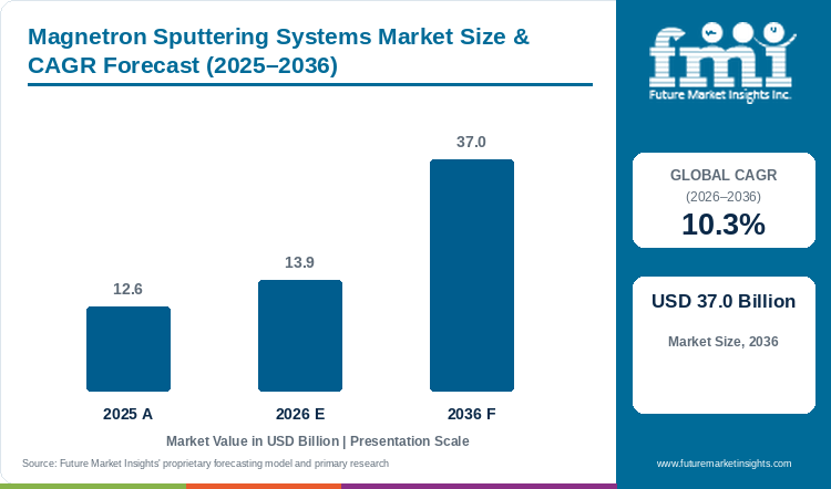
Demand for magnetron sputtering systems is projected to expand at 10.3% CAGR between 2026 and 2036. Industry value grows from USD 12.6 billion in 2025 to USD 13.9 billion in 2026 and is projected to reach USD 37.0 billion by 2036.
Magnetron sputtering systems gain wide adoption owing to their ability to deposit metal, barrier, seed and electrode films on semiconductor wafers alongside thin film coatings on precision microelectronics. As noted by FMI, the market was valued at USD 12.6 billion in 2025 and is projected to rise from USD 13.9 billion in 2026 to USD 37.0 billion by 2036, at 10.3% CAGR. Automated vacuum cluster tools held 46.9% of system architecture demand in 2026, as wafers move between connected chambers without repeated atmospheric exposure. The U.S. Government Accountability Office reported 40 semiconductor projects across 19 companies, backed by USD 30.9 billion in direct awards and USD 5.5 billion in loans during 2025.[1]
Key Market Trends & Insights
- By wafer size compatibility: 300 mm advanced-fab wafers led the market with a share of 44.7% in 2026, supported by high-volume fab throughput and maximum die output per processed substrate.
- By process node: Leading-edge sub-5 nm nodes accounted for 47.3% of revenue in 2026, driven by multi-layer barrier, seed, and electrode film requirements in advanced logic.
- By system architecture: Automated vacuum cluster tools represented 46.9% of demand in 2026, reflecting the need to transfer wafers between deposition and pre-clean modules without atmospheric exposure.
- By end user tier: Integrated device manufacturers held the leading share of 41.1% in 2026, underpinned by captive fabrication capacity and custom thin-film recipe control.
Regional Highlights
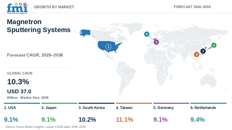
- Fastest-growing profiled country: Taiwan (11.1% CAGR, 2026 to 2036).
- By country: South Korea (10.2%) and the Netherlands (9.4%) follow, while the USA, Japan, and Germany record 9.1% CAGR.
Market Size & Forecast
Table 1: Market Size and Forecast for the Magnetron Sputtering Systems Market (USD billion and percentage), 2025 to 2036
| Metric | Value |
|---|---|
| 2025 Market Size | USD 12.6 billion |
| Estimated Market Size in 2026 | USD 13.9 billion |
| Projected Market Size by 2036 | USD 37.0 billion |
| CAGR, 2026 to 2036 | 10.3% |
| Added Revenue, 2026 to 2036 | USD 23.1 billion |
| Market Expansion Multiple | 2.7x |
Fab capacity alone does not decide how many magnetron sputtering systems are required. The number of film steps, production mix and chamber utilization also changes equipment demand. Texas Instruments started production at its newest 300 mm fab in December 2025, and the facility will ultimately produce tens of millions of chips every day.[2]
Fabrication Capacity and Tool Readiness
Fabrication investment explains only one part of sputtering system demand. Wafer output decides chamber use, whereas a wider product mix requires more recipes and process modules. Project milestones also decide when systems are installed and when targets, parts and field service are required. The indicators below connect these factors with demand for deposition chambers and related support.
Table 2: Fabrication Capacity and Tool Readiness Indicators for the Magnetron Sputtering Systems Market (projects, wafers, modules, products, technologies, customers, and percentages), mixed reporting years from 2025 to 2033
| Indicator | Data Point | Why It Matters | Source |
|---|---|---|---|
| U.S. funded projects | 40 projects across 19 companies | Projects cover materials, fabrication and packaging, widening the number of sites requiring deposition equipment. | [1] |
| TSMC managed wafer capacity | More than 17 million 12-inch-equivalent wafers in 2025 | Higher wafer output supports chamber utilization, target replacement and field service. | [13] |
| TSMC production diversity | 12,682 products; 305 technologies; 534 customers | A wider process mix increases recipe, module and qualification requirements. | [13] |
| Texas Instruments fab program | More than USD 60 billion; seven U.S. fabs; over 60,000 jobs | New 300 mm capacity creates demand for compatible production and service equipment. | [3] |
| ENTRON-EXX modularity | Up to 12 modules; 50% lower relocation and set-up time | Module additions allow a transfer platform to move from development into changing production requirements. | [5] |
| Funded project milestones | 24 of 161 reports completed by July 2025; final projects extend to 2033 | Equipment demand is likely to be released in stages as fabrication projects reach installation milestones. | [1] |
Analyst Perspective
“I expect advanced packaging to widen sputtering demand as larger formats requires additional seed, barrier and metal deposition stages. Cluster tools with stable chamber matching will gain preference when new fabs move from qualification into volume production.”
- Nikhil Kaitwade, Principal Consultant, Future Market Insights.
How is the magnetron sputtering systems market segmented?
Magnetron sputtering systems market is segmented by four primary commercial axes and region: wafer size compatibility, process node, system architecture, end user tier, and region. In 2026, 300 mm wafers are projected at 44.7%, sub-5 nm nodes at 47.3%, cluster tools at 46.9%, and IDMs at 41.1%.
By wafer size compatibility: 300 mm advanced-fab wafers, 200 mm legacy-fab wafers, and compound semiconductor substrates (SiC/GaN).
By process node: leading-edge sub-5 nm nodes, mature 7 nm to 28 nm nodes, and legacy power and discrete nodes.
By system architecture: automated vacuum cluster tools, in-line track systems, single-wafer processing chambers, and batch sputtering platforms.
By end user tier: integrated device manufacturers (IDMs), pure-play foundries, OSAT providers, and advanced R&D cleanrooms.
By region: North America, Latin America, Western Europe, Eastern Europe, East Asia, South Asia and Pacific, and Middle East and Africa.
Why do 300 mm wafers retain a notable compatibility share?
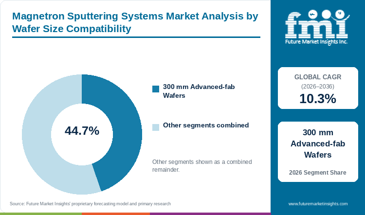
Based on wafer size compatibility, 300 mm advanced-fab wafers are projected to account for 44.7% in 2026, driven by fab-scale throughput.
Table 3: Wafer Size Compatibility Share for the Magnetron Sputtering Systems Market (percentage share), 2026
| Wafer Size Compatibility | Share (2026) |
|---|---|
| 300 mm Advanced-fab Wafers | 44.7% |
| Other Segments Combined | 55.3%* |
| Total | 100.0% |
*Calculated as the balance remaining after deducting the leading segment's reported share from 100.0%.
Table 4: Wafer Size Compatibility Leadership and Market Growth for the Magnetron Sputtering Systems Market (segment and CAGR percentage), 2026 to 2036
| Metric | Value |
|---|---|
| Global CAGR (2026 to 2036) | 10.3% |
| Leading Segment | 300 mm Advanced-fab Wafers |
Three-hundred-millimeter wafers produce more dies in one production cycle when compared with smaller wafer formats. Due to this output advantage, semiconductor manufacturers are installing cluster tools capable of processing these substrates alongside semiconductor wafer fabrication lines at higher throughput. According to FMI, 300 mm advanced-fab wafers will account for 44.7% of wafer size compatibility demand in 2026. Expansion of 300 mm fabrication capacity is expected to drive demand for compatible chambers and service equipment.
- The 300 mm advanced-fab wafer segment accounts for 44.7% share in 2026 owing to higher die output from each production cycle.
- In June 2025, Texas Instruments announced more than USD 60 billion investment for seven semiconductor fabs in Texas and Utah. The company stated that the plan will support over 60,000 jobs. These planned fabs include dependable 300 mm capacity which requires metal and barrier film deposition before commercial production.[3] Expansion of 300 mm production is anticipated to support demand for compatible sputtering chambers and service equipment.
What supports sub-5 nm nodes as a preferred process category?
In 2026, leading-edge sub-5 nm nodes are expected to lead process node revenue with 47.3% share, owing to complex metal stacks.
Leading-edge sub-5 nm devices requires thinner films and more controlled interfaces as wiring dimensions become smaller, requiring integration with chemical vapor deposition and atomic-scale processing stages. Barrier, liner, electrode and seed layers are deposited at different stages of device production. FMI research indicates that sub-5 nm nodes will account for 47.3% of process node revenue in 2026. Higher number of controlled metal layers is expected to support adoption of accurate sputtering systems.
- Leading-edge sub-5 nm nodes account for 47.3% share in 2026 due to increasing number of controlled metal layers.
- In April 2026, Applied Materials introduced deposition systems for angstrom-era logic chips and advanced interconnects.[4] These systems are directed towards gate-all-around transistors where controlled film thickness is required at smaller dimensions. Development of deposition equipment for advanced logic indicates increasing requirement for accurate interfaces. This is anticipated to support demand from sub-5 nm process lines.
How do cluster tools meet changing architecture requirements?
Automated vacuum cluster tools are set to lead system architecture with 46.9% share in 2026, enabled by controlled wafer transfer.
Automated vacuum cluster tools combine sputter chambers, pre-clean, heating and wafer transfer in one production system, operating in tandem with sputtering target materials to maintain uniform deposition. A wafer moves between these modules without repeated atmospheric exposure, due to which contamination between deposited layers can be reduced.
- Automated vacuum cluster tools account for 46.9% share in 2026 owing to controlled wafer movement between connected process chambers.
- In January 2025, ULVAC started accepting orders for the ENTRON-EXX multi-chamber deposition system for semiconductor applications.[5] The system provides equipment data functions and space for adding or changing process modules. This allows semiconductor manufacturers to use one transfer platform for development and mass production requirements.
Why do integrated device manufacturers anchor end-user demand?
Integrated device manufacturers are projected to hold 41.1% of end user tier demand in 2026, supported by captive process integration.
Integrated device manufacturers develop chip designs and produce them within their own fabrication facilities. These manufacturers can change deposition recipes, maintenance periods and process conditions according to each device requirement, often coordinating tool sets with high-k metal precursors for advanced transistor stacks.
- Integrated device manufacturers hold 41.1% share in 2026 owing to captive process development and production control.
- Germany Trade & Invest reported semiconductor revenue of more than USD 17 billion during 2025.[6] The organization also projected up to USD 40 billion in public and private spending by 2030. Presence of automotive, power and sensor chip manufacturers creates requirement for contacts, electrodes and adhesion layers. This is expected to support demand for magnetron sputtering systems among integrated device manufacturers.
What are the drivers, restraints, and opportunities in the magnetron sputtering systems market?
In the magnetron sputtering systems market, fab construction is the key driver, qualification cost is the key restraint, and compound-semiconductor capacity is the key opportunity.
- Driver: New wafer fabs and advanced packaging lines expand the installed base for sputter deposition.
- Restraint: Long process qualification and chamber-matching requirements can delay tool acceptance and revenue recognition.
- Opportunity: SiC, GaN, sensors, optics, and advanced packaging widen demand beyond leading-edge logic.
Fab Programs Expand Tool Demand
New wafer fabs requires metal, barrier, electrode and adhesion film deposition before volume production can begin. In July 2025, the Semiconductor Industry Association reported more than 100 semiconductor projects across 28 U.S. states, representing over USD 500 billion in private investment.[7] The projects may support more than 500,000 jobs as plants and related facilities are completed. Each fabrication line requires deposition chambers, targets, vacuum components and field service, complementing investments in advanced packaging technologies across leading-edge chipmaker facilities. Expansion of these projects is expected to drive the magnetron sputtering systems market growth.
Qualification Extends Purchase Cycles
Long process qualification is one of the primary factor limiting adoption of magnetron sputtering systems. Film thickness, particles, adhesion and chamber matching must meet the approved device requirement before production use. In January 2025, the Netherlands announced wider export authorization controls for specified measuring and inspection equipment used in advanced semiconductor production.[8] Export review along with equipment qualification can increase delivery and acceptance time, aligning with stringent qualification protocols seen across semiconductor inspection systems and metrology tools. These factors may hamper growth of the magnetron sputtering systems market.
Compound Devices Widen Applications
Compound semiconductor devices requires metal contacts, adhesion layers and barrier films on SiC and GaN substrates. A 2026 Germany Trade & Invest profile stated that more than one-third of European chips are produced in Germany.[9] Automotive electronics, power semiconductors, sensors and automation are supporting production of these devices. Use of sputtering equipment is therefore widening beyond advanced logic into power and sensor applications, driving broader adoption of compound semiconductor materials across power and automotive electronics. These applications are expected to create growth opportunities for magnetron sputtering system manufacturers.
Which country CAGRs are profiled in the magnetron sputtering systems market?
Table 5: Country CAGR Comparison for the Magnetron Sputtering Systems Market (CAGR percentage), 2026 to 2036
| Country | CAGR |
|---|---|
| USA | 9.1% |
| Japan | 9.1% |
| South Korea | 10.2% |
| Taiwan | 11.1% |
| Germany | 9.1% |
| Netherlands | 9.4% |
How do country-level CAGRs compare in the magnetron sputtering systems market?
Country demand is expected to remain higher where wafer capacity, memory output and advanced packaging investment is expanding. As per FMI, Taiwan and South Korea follow foundry and memory-led routes, whereas Western markets gain from fabs, equipment engineering and application-driven chips.
Taiwan and South Korea are projected to show stronger expansion owing to foundry and memory production. The USA combines funded fab projects with a large installed equipment base. Japan is rebuilding advanced-node capacity, while Germany and the Netherlands gain from application chips, equipment engineering and semiconductor research.
- USA demand follows 300 mm fab construction and funded supply-chain projects.
- Japan combines advanced-node rebuilding with a broad domestic materials and equipment base.
- South Korea connects memory investment with HBM and advanced packaging capacity.
- Taiwan maintains a high-volume foundry route and dense supplier support.
- Germany links deposition demand to automotive, power, sensor, and industrial chips.
- Netherlands demand remains tied to equipment engineering, metrology, and controlled global shipments.
Full report country CAGRs cover: North America; Latin America; Western Europe; Eastern Europe; East Asia; South Asia and Pacific; Middle East and Africa.
Country-wise Analysis
- The USA magnetron sputtering systems market is forecast to rise at 9.1% CAGR over the forecast period. In August 2026, the U.S. Government Accountability Office reported 49 semiconductor projects across 24 companies, with Commerce disbursing USD 13.1 billion under CHIPS for America funding.[10] Awardees had completed the required milestones by their due dates as of April 2026. However, some project work remained behind the planned schedule. New fabrication and packaging lines requires metal and barrier deposition before production is expanded, reinforcing demand for ALD precursors and thin-film equipment across funded domestic fabrication sites. Expansion of funded semiconductor projects is anticipated to support the USA market revenue growth.
- Japan magnetron sputtering systems market is anticipated to advance at 9.1% CAGR through 2036 owing to advanced-node production and local equipment supply. In November 2025, the International Trade Administration estimated Japan semiconductor market at USD 51.886 billion.[11] The government had provided more than USD 6.1 billion funding for Rapidus, which is planning 2 nm production in 2027. Advanced logic requires controlled metal films and interface deposition. Apart from logic chips, Japan produces memory, sensors and power devices that use sputtered contacts and electrodes. Availability of domestic equipment companies is expected to support transfer of pilot processes into fabrication lines, which will drive the Japan market growth.
- Adoption of magnetron sputtering systems in South Korea is estimated to expand at 10.2% CAGR through 2036. In March 2026, the national strategic-technology plan increased public research spending by 30% to USD 5.77 billion.[12] The plan covered 513 designated technologies including semiconductors and AI. South Korea has a large memory manufacturing base where sputtered metal and barrier layers are used at repeated stages. Expansion of HBM and advanced packaging is increasing use of seed and redistribution layer metallization. Presence of fabrication plants and equipment service networks is expected to support tool installation during the forecast period.
- By 2036, Taiwan is projected to grow at 11.1% CAGR owing to high-volume foundry capacity and advanced-node production. TSMC reported managed capacity of more than 17 million 12-inch-equivalent wafers in 2025, operating six 12-inch GIGAFAB facilities and four 8-inch fabs in Taiwan.[13] Due to this production network, sputtering demand remains close to large wafer output. Advanced logic uses adhesion, barrier, seed and electrode films at controlled thickness, often following wafer thinning executed on back grinding systems prior to 3D packaging assembly. Higher wafer output also increases target replacement and chamber service work. Continued foundry production is anticipated to propel demand for magnetron sputtering systems in Taiwan.
- Germany is estimated to post 9.1% CAGR over the forecast period owing to automotive, power and industrial semiconductor production. In March 2026, Germany selected 38 projects for the Advanced Semiconductor Technologies IPCEI.[14] The selected projects included AI chips and production facilities, while around one-third of participating companies were startups and SMEs. These project connects German companies with European partners for joint semiconductor value chains. Magnetron sputtering systems are required for metal contacts, sensor stacks and power-device layers. Expansion of application-driven semiconductor projects is expected to support the Germany market growth.
- Magnetron sputtering system sales in the Netherlands are forecast to expand at 9.4% CAGR through 2036 owing to equipment engineering and semiconductor research. In May 2025, the Dutch government stated that the five largest semiconductor companies generated around USD 50 billion in combined revenue.[15] The same report identified the Netherlands as an important part of the global semiconductor equipment chain. Export authorization can increase delivery planning time for controlled systems. However, local equipment, metrology and university networks supports module development and qualification. Continued engineering activity is anticipated to support the Netherlands magnetron sputtering systems market growth.
Who are the notable companies in the magnetron sputtering systems market?
Applied Materials, ULVAC, Canon Anelva, Tokyo Electron, VON ARDENNE, Buhler Leybold Optics, Veeco Instruments, Denton Vacuum, Angstrom Engineering, and Kurt J. Lesker Company are notable companies profiled in this market.
Magnetron sputtering systems market is moderately fragmented between production fab equipment, large-area coating systems and configurable research platforms. Applied Materials and ULVAC offers integrated systems and process modules for semiconductor fabs. Canon Anelva supplies equipment for logic, memory, sensors and packaging, whereas VON ARDENNE produces magnetrons for wafer, glass and optical coating. Specialist manufacturers focus on flexible chambers and smaller production systems. Some of the prominent players are expanding advanced packaging platforms and service networks in order to increase its customer base.
VON ARDENNE develops magnetrons in-house for wafer, glass, optics and large-area coating systems.[16] Specialist suppliers serve research laboratories and smaller production lines through flexible chamber configuration. Customer switching remains limited after a recipe is qualified on one platform, as the replacement system must reproduce the approved film result.
- Production semiconductor platforms: Applied Materials, ULVAC, Canon Anelva, and Tokyo Electron.
- Large-area and optical coating systems: VON ARDENNE and Buhler Leybold Optics.
- Specialist deposition platforms: Veeco Instruments, Denton Vacuum, Angstrom Engineering, and Kurt J. Lesker Company.
Competitive Benchmarking: Magnetron Sputtering Systems Market
Table 6: Competitive Benchmarking for the Magnetron Sputtering Systems Market (qualitative capability ratings), 2026
| Company | Platform breadth | Process depth | Current activity | Geographic reach |
|---|---|---|---|---|
| Applied Materials | High | High | High | High |
| ULVAC | High | High | High | High |
| Canon Anelva | High | Medium | High | Medium |
| Tokyo Electron | High | High | High | High |
| VON ARDENNE | High | High | Medium | High |
| Buhler Leybold Optics | Medium | High | Medium | High |
| Veeco Instruments | Medium | Medium | High | High |
| Denton Vacuum | Medium | Medium | Medium | Medium |
| Angstrom Engineering | Medium | Medium | Medium | Medium |
| Kurt J. Lesker Company | Medium | Medium | Medium | High |
High rating indicates wider product portfolio, process capability, present company activity and geographic reach. Medium rating indicates established but narrower evidence. Low rating indicates limited direct evidence. These ratings do not represent market share, product quality or company ranking.
Key Developments in the Magnetron Sputtering Systems Market
- In June 2026, Applied Materials introduced systems for DRAM and advanced packaging, extending materials engineering across deposition and process control.[17]
- In May 2026, Applied Materials agreed to acquire the NEXX business to broaden panel-level advanced packaging deposition capability.[18]
- In April 2026, ULVAC stated that the US-JOINT semiconductor packaging consortium began full operations in Silicon Valley with 12 participating companies.[19]
- In January 2025, ULVAC launched the ENTRON-EXX multi-chamber deposition system for semiconductor applications.
Key Players in the Magnetron Sputtering Systems Market
Integrated Semiconductor Production Platforms
- Applied Materials
- ULVAC
- Canon Anelva
- Tokyo Electron
Large-area and Optical Coating Platforms
- VON ARDENNE
- Buhler Leybold Optics
Research and Flexible Deposition Platforms
- Veeco Instruments
- Denton Vacuum
- Angstrom Engineering
- Kurt J. Lesker Company
Magnetron Sputtering Systems Market - Report Scope
Table 7: Report Scope for the Magnetron Sputtering Systems Market (coverage fields and definitions), 2026 to 2036
| Coverage field | Report scope |
|---|---|
| Market breakdown | Wafer size compatibility; process node; system architecture; end user tier; region |
| Quantitative units | USD billion |
| Market definition | First-sale revenue from magnetron sputtering systems, integrated chambers, cathodes supplied with systems, and directly linked control modules. Standalone target materials, general vacuum pumps, contract coating services, and unrelated PVD technologies are excluded. |
| Regions covered | North America; Latin America; Western Europe; Eastern Europe; East Asia; South Asia and Pacific; Middle East and Africa |
| Countries covered | USA; Japan; South Korea; Taiwan; Germany; Netherlands |
| Key companies profiled | Applied Materials, ULVAC, Canon Anelva, Tokyo Electron, VON ARDENNE, Buhler Leybold Optics, Veeco Instruments, Denton Vacuum, Angstrom Engineering, Kurt J. Lesker Company |
| Forecast period | 2026 to 2036 |
| Approach | Hybrid bottom-up and top-down sizing that reconciles equipment shipments, fab investment, installed systems, application mix, and country demand within the defined revenue boundary. |
Magnetron Sputtering Systems Market - Research Methodology
Table 8: Research Methodology for the Magnetron Sputtering Systems Market (research methods and approach), 2026 edition
| Method | Approach |
|---|---|
| Primary Research | The research study includes primary interviews with manufacturers, technology developers, distributors, end users, procurement teams and industry experts. Interviews covers purchasing decision, equipment evaluation, pricing, adoption barriers and technical support requirement. |
| Desk Research | Desk research includes government publications, regulatory records, trade data, industry associations, company filings and official product information. Sources are checked for publication date, geographic coverage and direct relevance to magnetron sputtering systems market. |
| Market Sizing and Forecasting | Market sizing combines base-year value, equipment shipment, installed systems, application demand, pricing, company participation and country demand. Forecast considers fabrication investment, technology adoption, purchasing cycle, equipment availability and barriers affecting wider use. |
| Data Validation | Market estimates are checked with government data, company activity, trade patterns and primary research findings. Overlapping revenue, unrelated PVD equipment and activities outside the market definition are excluded. |
Magnetron Sputtering Systems Market by Segments
Wafer Size Compatibility
- 300 mm Advanced-fab Wafers
- 200 mm Legacy-fab Wafers
- Compound Semiconductor Substrates (SiC/GaN)
Process Node
- Leading-edge Sub-5 nm Nodes
- Mature 7 nm to 28 nm Nodes
- Legacy Power and Discrete Nodes
System Architecture
- Automated Vacuum Cluster Tools
- In-line Track Systems
- Single-wafer Processing Chambers
- Batch Sputtering Platforms
End User Tier
- Integrated Device Manufacturers (IDMs)
- Pure-play Foundries
- OSAT Providers
- Advanced R&D Cleanrooms
Magnetron Sputtering Systems Market by Region
- North America
- United States
- Canada
- Latin America
- Brazil
- Mexico
- Argentina
- Chile
- Western Europe
- Germany
- France
- United Kingdom
- Italy
- Spain
- Benelux
- Nordics
- Eastern Europe
- Poland
- Czech Republic
- Romania
- Hungary
- East Asia
- Japan
- South Korea
- Taiwan
- South Asia and Pacific
- ASEAN
- Australia and New Zealand
- Middle East and Africa
- GCC Countries
- South Africa
- Turkiye
- Israel
Research Sources and Bibliography
- [1] U.S. Government Accountability Office. (2025, December). Semiconductors: Information on projects funded to strengthen U.S. supply chain.
- [2] Texas Instruments. (2025, December 17). Texas Instruments begins production at its newest 300 mm semiconductor manufacturing facility in Sherman, Texas.
- [3] Texas Instruments. (2025, June 18). Texas Instruments plans to invest more than USD 60 billion to manufacture billions of foundational semiconductors in the U.S..
- [4] Applied Materials, Inc. (2026, April 8). Applied Materials introduces deposition systems for angstrom-era logic chips.
- [5] ULVAC Technologies, Inc. (2025, January 20). ULVAC launches new deposition system for semiconductor applications: Model ENTRON-EXX.
- [6] Germany Trade & Invest. (2026). Semiconductor industry in Germany.
- [7] Semiconductor Industry Association. (2025, July). State of the U.S. semiconductor industry 2025.
- [8] Government of the Netherlands. (2025, January 15). Export controls on advanced semiconductor manufacturing equipment to be tightened.
- [9] Germany Trade & Invest. (2026, July). The semiconductor market in Germany: Issue 2026.
- [10] U.S. Government Accountability Office. (2026, August 6). Semiconductors: Commerce needs plan to meet CHIPS for America R&D requirements.
- [11] International Trade Administration. (2025, November 20). Japan: Semiconductors.
- [12] Ministry of Science and ICT, Republic of Korea. (2026, March 13). 2026 implementation plan for national strategic technologies.
- [13] Taiwan Semiconductor Manufacturing Company Limited. (2026). Fab capacity and 2025 annual report.
- [14] Germany Trade & Invest. (2026, March 19). Germany selects 38 projects for chipmaking IPCEI.
- [15] Government of the Netherlands. (2025, May 27). Progress report on the semiconductor industry in a changing geopolitical climate.
- [16] VON ARDENNE GmbH. (2026). Magnetron sputtering: Proven plasma technology for homogeneous coatings.
- [17] Applied Materials, Inc. (2026, June 25). New systems to accelerate DRAM and advanced packaging for AI chips.
- [18] Applied Materials, Inc. (2026, May 3). Applied Materials broadens advanced packaging portfolio with acquisition of NEXX.
- [19] ULVAC, Inc. (2026, April 21). USA-Japan semiconductor packaging consortium US-JOINT begins operations in Silicon Valley.
- [20] Applied Materials, Inc. (2026, October 1). Applied Materials and Besi expand strategic partnership to advance next-generation packaging for AI scaling.
- [21] Applied Materials, Inc. (2026, September 29). Applied Materials and KIOXIA partner at the EPIC Center to advance next-generation memory technology.
- [22] Applied Materials, Inc. (2026, June 10). Applied Materials expands Singapore manufacturing to support AI chip demand.
This bibliography is provided for reader reference. The full report contains the complete reference list and detailed citations.
This Report Answers
- How large is the magnetron sputtering systems market during 2026?
- What market value is projected for magnetron sputtering systems by 2036?
- Which wafer size compatibility segment holds notable share in 2026?
- Which system architecture holds a notable market share during 2026?
- Which countries show notable magnetron sputtering systems expansion outlooks?
- Which companies are notable in the magnetron sputtering systems market?
Frequently Asked Questions
How large is the magnetron sputtering systems market in 2026?
Future Market Insights estimates that the magnetron sputtering systems market will be valued at USD 13.9 billion in 2026. New wafer fabs and repeated metal deposition stages are expected to take the market to USD 37.0 billion by 2036.
What CAGR is projected for the magnetron sputtering systems market?
As per FMI, the magnetron sputtering systems market is projected to grow at a 10.3% CAGR from 2026 to 2036. Growth is supported by 300 mm capacity, advanced-node metal films and expanding use of cluster tools.
Which wafer size compatibility segment leads the market in 2026?
Systems for 300 mm advanced-fab wafers are projected to hold 44.7% share in 2026. The segment benefits from high-throughput production and continued installation of 300 mm fabrication capacity.
Which system architecture holds a leading share in 2026?
Automated vacuum cluster tools are estimated to account for 46.9% share in 2026. Demand is supported by controlled wafer transfer between deposition, cleaning and heating modules.
Which country has a notable growth outlook through 2036?
Taiwan is projected to register an 11.1% CAGR from 2026 to 2036. Growth is supported by high-volume foundry capacity and continued advanced-node production.
Who are the key companies in the magnetron sputtering systems market?
Key participants include Applied Materials, ULVAC, Canon Anelva, Tokyo Electron, VON ARDENNE and Buhler Leybold Optics. These companies are focusing on multi-chamber systems, advanced packaging and application-specific deposition platforms.
Preview the report firsthand - request a free sample
Get SampleGet the brochure for pricing and purchase details.
Get PDFTable of Content
- Key Takeaways
- Market Size and CAGR
- Top Growth Driver
- Fastest Growing Segment
- Leading Region
- Key Companies
- Emerging Opportunities
- Executive Summary
- Global Market Outlook
- Demand-side Trends
- Supply-side Trends
- Technology Roadmap Analysis
- Analysis and Recommendations
- Analyst Perspective (What is happening? Why now? What should investors know?)
- Key Questions Answered
- How large is the market?
- What is the CAGR?
- What are key trends?
- Which region dominates?
- Who are the leaders?
- Market Overview
- Market Coverage / Taxonomy
- Market Definition / Scope / Limitations
- Research Methodology
- Chapter Orientation
- Analytical Lens and Working Hypotheses
- Market Structure, Signals, and Trend Drivers
- Benchmarking and Cross-market Comparability
- Market Sizing, Forecasting, and Opportunity Mapping
- Research Design and Evidence Framework
- Desk Research Programme (Secondary Evidence)
- Expert Input and Fieldwork (Primary Evidence)
- Tooling, Models, and Reference Databases
- Data Engineering and Model Build
- Quality Assurance and Audit Trail
- Market Background
- Market Dynamics (Drivers, Restraints, Opportunity, Trends)
- Scenario Forecast (Optimistic, Likely, Conservative)
- Impact Analysis
- AI Impact
- Sustainability Impact
- Regulatory Impact
- Technology Impact
- Consumer / Buyer Analysis
- Purchase Drivers
- Adoption Barriers
- Buyer Journey
- Opportunity Map Analysis
- Product Life Cycle Analysis
- Supply Chain Analysis
- Investment Feasibility Matrix
- Value Chain Analysis
- PESTLE and Porter's Analysis
- Regulatory Landscape
- Regional Parent Market Outlook
- Production and Consumption Statistics
- Import and Export Statistics
- Global Market Analysis and Forecast, 2021 to 2036
- Historical Market Size Value (USD Billion) Analysis, 2021 to 2025
- Current and Future Market Size Value (USD Billion) Projections, 2026 to 2036
- Y-o-Y Growth Trend Analysis
- Absolute $ Opportunity Analysis
- Global Market Pricing Analysis, 2021 to 2036
- Global Market Analysis and Forecast, By Wafer Size Compatibility, 2021 to 2036
- Introduction / Key Findings
- Historical Market Size Value (USD Billion) Analysis By Wafer Size Compatibility, 2021 to 2025
- Current and Future Market Size Value (USD Billion) Analysis and Forecast By Wafer Size Compatibility, 2026 to 2036
- 300 mm Advanced-fab Wafers
- 200 mm Legacy-fab Wafers
- Compound Semiconductor Substrates (SiC/GaN)
- Y-o-Y Growth Trend Analysis By Wafer Size Compatibility, 2021 to 2025
- Absolute $ Opportunity Analysis By Wafer Size Compatibility, 2026 to 2036
- Global Market Analysis and Forecast, By Process Node, 2021 to 2036
- Introduction / Key Findings
- Historical Market Size Value (USD Billion) Analysis By Process Node, 2021 to 2025
- Current and Future Market Size Value (USD Billion) Analysis and Forecast By Process Node, 2026 to 2036
- Leading-edge Sub-5 nm Nodes
- Mature 7 nm to 28 nm Nodes
- Legacy Power and Discrete Nodes
- Y-o-Y Growth Trend Analysis By Process Node, 2021 to 2025
- Absolute $ Opportunity Analysis By Process Node, 2026 to 2036
- Global Market Analysis and Forecast, By System Architecture, 2021 to 2036
- Introduction / Key Findings
- Historical Market Size Value (USD Billion) Analysis By System Architecture, 2021 to 2025
- Current and Future Market Size Value (USD Billion) Analysis and Forecast By System Architecture, 2026 to 2036
- Automated Vacuum Cluster Tools
- In-line Track Systems
- Single-wafer Processing Chambers
- Batch Sputtering Platforms
- Y-o-Y Growth Trend Analysis By System Architecture, 2021 to 2025
- Absolute $ Opportunity Analysis By System Architecture, 2026 to 2036
- Global Market Analysis and Forecast, By End User Tier, 2021 to 2036
- Introduction / Key Findings
- Historical Market Size Value (USD Billion) Analysis By End User Tier, 2021 to 2025
- Current and Future Market Size Value (USD Billion) Analysis and Forecast By End User Tier, 2026 to 2036
- Integrated Device Manufacturers (IDMs)
- Pure-play Foundries
- OSAT Providers
- Advanced R&D Cleanrooms
- Y-o-Y Growth Trend Analysis By End User Tier, 2021 to 2025
- Absolute $ Opportunity Analysis By End User Tier, 2026 to 2036
- Global Market Analysis and Forecast, By Region, 2021 to 2036
- Introduction
- Historical Market Size Value (USD Billion) Analysis By Region, 2021 to 2025
- Current Market Size Value (USD Billion) Analysis and Forecast By Region, 2026 to 2036
- North America
- Latin America
- Western Europe
- Eastern Europe
- East Asia
- South Asia and Pacific
- Middle East and Africa
- Market Attractiveness Analysis By Region
- North America Market Analysis and Forecast, By Country, 2021 to 2036
- Historical Market Size Value (USD Billion) Trend Analysis By Market Taxonomy, 2021 to 2025
- Market Size Value (USD Billion) Forecast By Market Taxonomy, 2026 to 2036
- By Country
- United States
- Canada
- By Wafer Size Compatibility
- By Process Node
- By System Architecture
- By End User Tier
- By Country
- Market Attractiveness Analysis
- By Country
- By Wafer Size Compatibility
- By Process Node
- By System Architecture
- By End User Tier
- Key Takeaways
- Latin America Market Analysis and Forecast, By Country
- Historical Market Size Value (USD Billion) Trend Analysis By Market Taxonomy, 2021 to 2025
- Market Size Value (USD Billion) Forecast By Market Taxonomy, 2026 to 2036
- By Country
- Brazil
- Mexico
- Argentina
- Chile
- By Wafer Size Compatibility
- By Process Node
- By System Architecture
- By End User Tier
- By Country
- Market Attractiveness Analysis
- By Country
- By Wafer Size Compatibility
- By Process Node
- By System Architecture
- By End User Tier
- Key Takeaways
- Western Europe Market Analysis and Forecast, By Country
- Historical Market Size Value (USD Billion) Trend Analysis By Market Taxonomy, 2021 to 2025
- Market Size Value (USD Billion) Forecast By Market Taxonomy, 2026 to 2036
- By Country
- Germany
- France
- United Kingdom
- Italy
- Spain
- Benelux
- Nordics
- By Wafer Size Compatibility
- By Process Node
- By System Architecture
- By End User Tier
- By Country
- Market Attractiveness Analysis
- By Country
- By Wafer Size Compatibility
- By Process Node
- By System Architecture
- By End User Tier
- Key Takeaways
- Eastern Europe Market Analysis and Forecast, By Country
- Historical Market Size Value (USD Billion) Trend Analysis By Market Taxonomy, 2021 to 2025
- Market Size Value (USD Billion) Forecast By Market Taxonomy, 2026 to 2036
- By Country
- Poland
- Czech Republic
- Romania
- Hungary
- By Wafer Size Compatibility
- By Process Node
- By System Architecture
- By End User Tier
- By Country
- Market Attractiveness Analysis
- By Country
- By Wafer Size Compatibility
- By Process Node
- By System Architecture
- By End User Tier
- Key Takeaways
- East Asia Market Analysis and Forecast, By Country
- Historical Market Size Value (USD Billion) Trend Analysis By Market Taxonomy, 2021 to 2025
- Market Size Value (USD Billion) Forecast By Market Taxonomy, 2026 to 2036
- By Country
- Japan
- South Korea
- Taiwan
- By Wafer Size Compatibility
- By Process Node
- By System Architecture
- By End User Tier
- By Country
- Market Attractiveness Analysis
- By Country
- By Wafer Size Compatibility
- By Process Node
- By System Architecture
- By End User Tier
- Key Takeaways
- South Asia and Pacific Market Analysis and Forecast, By Country
- Historical Market Size Value (USD Billion) Trend Analysis By Market Taxonomy, 2021 to 2025
- Market Size Value (USD Billion) Forecast By Market Taxonomy, 2026 to 2036
- By Country
- ASEAN
- Australia and New Zealand
- By Wafer Size Compatibility
- By Process Node
- By System Architecture
- By End User Tier
- By Country
- Market Attractiveness Analysis
- By Country
- By Wafer Size Compatibility
- By Process Node
- By System Architecture
- By End User Tier
- Key Takeaways
- Middle East and Africa Market Analysis and Forecast, By Country
- Historical Market Size Value (USD Billion) Trend Analysis By Market Taxonomy, 2021 to 2025
- Market Size Value (USD Billion) Forecast By Market Taxonomy, 2026 to 2036
- By Country
- GCC Countries
- South Africa
- Turkiye
- Israel
- By Wafer Size Compatibility
- By Process Node
- By System Architecture
- By End User Tier
- By Country
- Market Attractiveness Analysis
- By Country
- By Wafer Size Compatibility
- By Process Node
- By System Architecture
- By End User Tier
- Key Takeaways
- Key Countries Market Analysis
- United States
- Pricing Analysis
- Market Share Analysis, 2025
- By Wafer Size Compatibility
- By Process Node
- By System Architecture
- By End User Tier
- Canada
- Pricing Analysis
- Market Share Analysis, 2025
- By Wafer Size Compatibility
- By Process Node
- By System Architecture
- By End User Tier
- Mexico
- Pricing Analysis
- Market Share Analysis, 2025
- By Wafer Size Compatibility
- By Process Node
- By System Architecture
- By End User Tier
- Brazil
- Pricing Analysis
- Market Share Analysis, 2025
- By Wafer Size Compatibility
- By Process Node
- By System Architecture
- By End User Tier
- Chile
- Pricing Analysis
- Market Share Analysis, 2025
- By Wafer Size Compatibility
- By Process Node
- By System Architecture
- By End User Tier
- Germany
- Pricing Analysis
- Market Share Analysis, 2025
- By Wafer Size Compatibility
- By Process Node
- By System Architecture
- By End User Tier
- United Kingdom
- Pricing Analysis
- Market Share Analysis, 2025
- By Wafer Size Compatibility
- By Process Node
- By System Architecture
- By End User Tier
- Italy
- Pricing Analysis
- Market Share Analysis, 2025
- By Wafer Size Compatibility
- By Process Node
- By System Architecture
- By End User Tier
- Spain
- Pricing Analysis
- Market Share Analysis, 2025
- By Wafer Size Compatibility
- By Process Node
- By System Architecture
- By End User Tier
- France
- Pricing Analysis
- Market Share Analysis, 2025
- By Wafer Size Compatibility
- By Process Node
- By System Architecture
- By End User Tier
- ASEAN
- Pricing Analysis
- Market Share Analysis, 2025
- By Wafer Size Compatibility
- By Process Node
- By System Architecture
- By End User Tier
- Australia and New Zealand
- Pricing Analysis
- Market Share Analysis, 2025
- By Wafer Size Compatibility
- By Process Node
- By System Architecture
- By End User Tier
- Japan
- Pricing Analysis
- Market Share Analysis, 2025
- By Wafer Size Compatibility
- By Process Node
- By System Architecture
- By End User Tier
- South Korea
- Pricing Analysis
- Market Share Analysis, 2025
- By Wafer Size Compatibility
- By Process Node
- By System Architecture
- By End User Tier
- Poland
- Pricing Analysis
- Market Share Analysis, 2025
- By Wafer Size Compatibility
- By Process Node
- By System Architecture
- By End User Tier
- Hungary
- Pricing Analysis
- Market Share Analysis, 2025
- By Wafer Size Compatibility
- By Process Node
- By System Architecture
- By End User Tier
- South Africa
- Pricing Analysis
- Market Share Analysis, 2025
- By Wafer Size Compatibility
- By Process Node
- By System Architecture
- By End User Tier
- Taiwan
- Pricing Analysis
- Market Share Analysis, 2025
- By Wafer Size Compatibility
- By Process Node
- By System Architecture
- By End User Tier
- Netherlands
- Pricing Analysis
- Market Share Analysis, 2025
- By Wafer Size Compatibility
- By Process Node
- By System Architecture
- By End User Tier
- United States
- Market Structure Analysis
- Competition Dashboard
- Competition Benchmarking
- Market Share Analysis of Top Players
- By Regional
- By Wafer Size Compatibility
- By Process Node
- By System Architecture
- By End User Tier
- Emerging Startups
- Innovation Benchmarking
- Competition Analysis
- Competition Deep Dive
- Applied Materials
- Overview
- Product Portfolio
- Profitability by Market Segments
- Sales Footprint
- Strategy Overview
- Marketing Strategy
- Product Strategy
- Channel Strategy
- ULVAC
- Canon Anelva
- Tokyo Electron
- VON ARDENNE
- Buhler Leybold Optics
- Veeco Instruments
- Denton Vacuum
- Angstrom Engineering
- Kurt J. Lesker Company
- Applied Materials
- Case Studies
- Success Stories
- Recent Developments
- Competition Deep Dive
- Assumptions & Acronyms Used