The 3D IC and 2.5D IC packaging market is projected to grow at a CAGR of 9.0% from 2025 to 2035, with the market anticipated at USD 58.3 billion in 2025 and forecast to reach USD 138.0 billion by 2035. Compound Absolute Growth Analysis shows an incremental expansion of nearly USD 79.7 billion over the ten-year span, driven by mounting demand for high-performance computing, artificial intelligence accelerators, and next-generation memory stacking.
Early growth between 2025 and 2029, where the market advances from USD 58.3 billion to USD 75.5 billion, indicates steady adoption as foundries refine through-silicon-via (TSV) technology and enhance yield rates. The later growth phase, from 2030 to 2035, is steeper, adding nearly USD 48.3 billion as chipmakers scale heterogeneous integration, integrating logic, memory, and sensors into single packages to meet the requirements of edge computing, 5G, and automotive electronics.
The compound nature of the growth curve highlights not only cumulative revenue but also the acceleration of adoption as process maturity reduces cost barriers. The market’s trajectory demonstrates how packaging technology has transitioned from experimental scaling to a mainstream enabler of advanced computing, where absolute dollar sales gains outpace earlier phases, ensuring sustained share expansion across multiple industries.
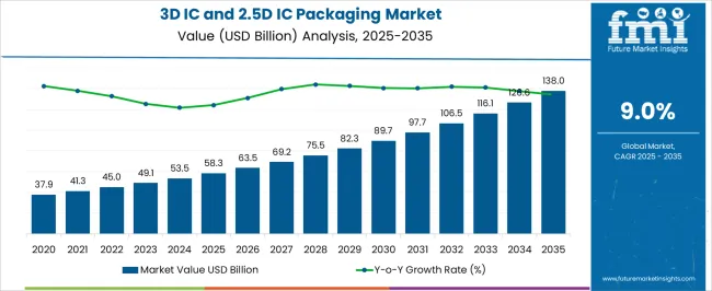
| Metric | Value |
|---|---|
| 3D IC and 2.5D IC Packaging Market Estimated Value in (2025 E) | USD 58.3 billion |
| 3D IC and 2.5D IC Packaging Market Forecast Value in (2035 F) | USD 138.0 billion |
| Forecast CAGR (2025 to 2035) | 9.0% |
The 3D IC and 2.5D IC packaging market is strongly influenced by five interconnected parent markets, each playing a critical role in shaping overall growth and adoption. The high-performance computing and data center segment holds the largest share at 38%, fueled by demand for advanced processors, GPUs, and memory stacking required for AI training, cloud services, and simulation workloads.
The consumer electronics sector contributes 25%, as smartphones, tablets, and wearables increasingly rely on compact, energy-efficient packaging technologies to enhance performance and reduce footprint. The automotive and mobility segment accounts for 15%, with autonomous driving systems, ADAS modules, and infotainment platforms driving adoption of heterogeneous integration solutions. The networking and 5G infrastructure sector represents 12% where demand is driven by low-latency, high-bandwidth devices needing reliable interconnects and miniaturized designs. The industrial and IoT applications segment holds a 10 percent share, focusing on sensors, edge computing, and industrial automation systems requiring optimized form factors and thermal efficiency.
Data centers, consumer electronics, and automotive segments capture nearly 80% of total demand, underscoring the dominance of performance-driven and energy-efficient applications. The future of 3D IC and 2.5D IC packaging lies in balancing cost, scale, and system-level reliability, with data-intensive industries setting the pace for adoption while IoT and networking provide additional growth pathways.
The 3D IC and 2.5D IC packaging market is experiencing significant expansion due to the increasing demand for miniaturization and enhanced performance in semiconductor devices. The market growth is being propelled by the rising need for higher bandwidth, improved power efficiency, and reduced latency in electronics.
These advanced packaging technologies enable the stacking and integration of multiple chips within a single package, which supports the development of compact, high-functioning devices used in consumer electronics, data centers, and telecommunications. Innovations in interconnect technology and thermal management are further facilitating the adoption of these packaging solutions.
The market outlook remains strong as emerging applications in artificial intelligence, 5G communications, and automotive electronics continue to drive the demand for sophisticated packaging methods that can accommodate complex chip architectures and deliver superior performance.
The 3d ic and 2.5d ic packaging market is segmented by technology, application, end use, and geographic regions. By technology, 3d ic and 2.5d ic packaging market is divided into 3D TSV, 3D wafer-level chip-scale packaging, and 2.5D. In terms of application, 3d ic and 2.5d ic packaging market is classified into Logic, Memory, Imaging & optoelectronics, MEMS/Sensors, LED, and Others. Based on end use, 3d ic and 2.5d ic packaging market is segmented into Consumer electronics, Telecommunication, Automotive, Military & aerospace, Medical devices, Smart technologies, and Others. Regionally, the 3d ic and 2.5d ic packaging industry is classified into North America, Latin America, Western Europe, Eastern Europe, Balkan & Baltic Countries, Russia & Belarus, Central Asia, East Asia, South Asia & Pacific, and the Middle East & Africa.
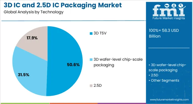
The 3D TSV technology segment is projected to hold 50.6% of the market revenue share in 2025, making it the leading technology type in the 3D IC and 2.5D IC packaging market. This position is being attributed to the superior vertical integration capabilities of 3D TSV, which enables high-density interconnects and reduces the length of inter-chip connections, thereby improving signal integrity and power efficiency.
The technology has found widespread acceptance in applications demanding compact and high-performance chip packages. Its ability to support heterogeneous integration of different chip types has further accelerated its adoption.
Additionally, advancements in TSV fabrication processes have enhanced yield and reduced costs, making this technology more accessible for mass production.
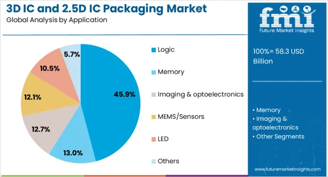
The logic application segment is expected to capture 45.9% of the market revenue share in 2025, leading all application categories. The growth of this segment is being driven by the increasing complexity and performance requirements of logic chips used in processors and microcontrollers.
Logic applications benefit significantly from 3D and 2.5D packaging due to the enhanced data transfer rates and lower power consumption that these packaging methods provide. The demand for high-performance computing and mobile devices has further fueled the adoption of advanced packaging solutions in logic applications.
The ability to integrate memory and logic components within a single package supports performance optimization and space savings, which are critical factors in the continued expansion of this segment.
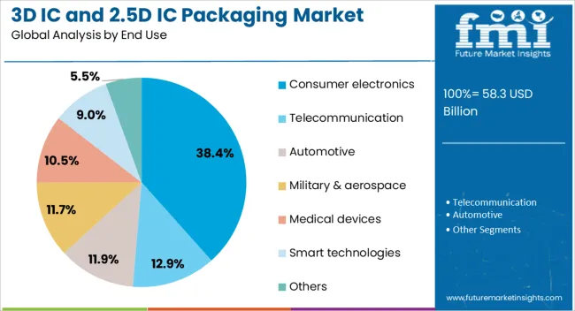
The consumer electronics end-use industry segment is projected to hold 38.4% of the market revenue share in 2025, making it the largest end-use sector in the 3D IC and 2.5D IC packaging market. This leadership is being attributed to the rapid proliferation of smartphones, tablets, wearable devices, and other portable electronics that demand miniaturized and high-performance semiconductor components.
The consumer electronics industry favors packaging technologies that enable compact designs while delivering improved speed and energy efficiency. As consumer expectations for device functionality and form factor continue to rise, the adoption of 3D and 2.5D packaging solutions has been accelerated.
Furthermore, the need for cost-effective manufacturing and faster time-to-market has encouraged manufacturers to embrace these packaging technologies in consumer electronics production lines.
The 3D IC and 2.5D IC packaging market is shaped by high-performance computing, consumer electronics adoption, automotive applications, and cost-supply dynamics. Growth will accelerate as integration density and efficiency remain decisive levers.
The 3D IC and 2.5D IC packaging sector is heavily shaped by increasing reliance on high-performance computing. Data centers, AI accelerators, and enterprise cloud workloads demand compact, thermally efficient packages that deliver high bandwidth and low latency. The transition from conventional packaging to stacked dies and interposers has been reinforced by exponential growth in AI and machine learning models that require faster memory access. The compound annual growth shows that integration density and reduced power consumption are not just technological shifts but commercial necessities. This dynamic anchors the market firmly in the enterprise computing ecosystem, where workload optimization dictates rapid adoption of advanced packaging solutions.
Consumer electronics continues to strengthen its role as a major driver of 3D IC and 2.5D IC packaging. Smartphones, tablets, AR/VR devices, and wearables are increasingly built with stacked memory and interposer-based designs to reduce footprint while improving efficiency. This evolution ensures better graphics performance, faster processing, and superior thermal handling for compact devices. Companies focus on advanced packaging to differentiate in a saturated electronics market, making integration density a competitive necessity. Shift from traditional single-die packages to 3D structures is no longer an optional strategy but an inevitable outcome of consumer preferences for high-speed, low-power, and feature-rich devices.
The automotive industry plays a crucial role in the adoption of 3D IC and 2.5D IC packaging. Advanced driver assistance systems, autonomous driving platforms, and infotainment modules demand higher computational capacity, which 3D stacking and interposers provide efficiently. These systems require lower power footprints while ensuring reliability in harsh operating conditions. Automotive OEMs are integrating advanced packaging to handle sensor fusion, real-time data analytics, and in-vehicle connectivity. This dynamic positions automotive applications as a transformative growth avenue where safety, efficiency, and processing speed converge. Long-term adoption will be driven by regulations supporting vehicle automation and electrification strategies globally.
Despite growth momentum, the 3D IC and 2.5D IC packaging sector faces constraints from cost structures, yield management, and supply chain complexities. Yield losses in through-silicon-via processes and thermal management costs elevate production challenges. Suppliers focus on modular interposers and improved assembly methods to lower costs. Regional dependence on advanced fabs creates vulnerabilities, as geopolitical and material shortages can delay adoption. Yet, these challenges also drive differentiation where companies mastering process yield and cost reduction secure a premium advantage. The ability to address these barriers through partnerships, scale economies, and advanced testing will define market leaders and their long-term profitability.
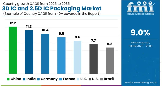
| Country | CAGR |
|---|---|
| China | 12.2% |
| India | 11.3% |
| Germany | 10.4% |
| France | 9.5% |
| UK | 8.6% |
| USA | 7.7% |
| Brazil | 6.8% |
The global 3D IC and 2.5D IC packaging market is projected to grow at a CAGR of 9.0% from 2025 to 2035. China leads at 12.2%, followed by India at 11.3%, Germany at 10.4%, France at 9.5%, the UK at 8.6%, and the USA at 7.7%. Growth is driven by strong adoption of heterogeneous integration, AI accelerators, memory stacking, and advanced chiplet designs that deliver higher bandwidth and lower power consumption. Asia-Pacific, particularly China and India, demonstrates rapid expansion through semiconductor manufacturing capacity, government-led incentives, and domestic electronics consumption. Germany and France emphasize automotive electronics, industrial automation, and high-efficiency computing, while the UK expands through design leadership and collaborative R&D hubs. The USA focuses on AI computing, defense applications, and large-scale data center integration, maintaining steady but competitive growth. Foundry partnerships, packaging innovation, and end-use diversification further enhance dollar sales and market share. The analysis includes over 40+ countries, with the leading markets highlighted above.
The 3D IC and 2.5D IC packaging market in China is projected to grow at a CAGR of 12.2% from 2025 to 2035, supported by strong government-led semiconductor policies, expanding foundry capabilities, and large-scale consumer electronics production. Chinese firms are investing heavily in through-silicon-via (TSV) technology and advanced interposers, allowing them to compete with global leaders in chiplet integration. Rapid adoption is being observed across AI, high-performance computing, and 5G infrastructure, where performance density and power efficiency are critical. Domestic partnerships with cloud service providers and international technology firms strengthen China’s global supply chain footprint. China’s scale, combined with its policy-driven push for semiconductor independence, positions it as the leading market globally.
The 3D IC and 2.5D IC packaging market in India is expected to grow at a CAGR of 11.3% between 2025 and 2035, driven by surging demand in consumer electronics, telecom infrastructure, and renewable-linked digital grids. Domestic semiconductor programs such as “Make in India” are encouraging foundry development and localized assembly. India’s IT and data center industry provides an expanding base for advanced packaging adoption, while global players are partnering with Indian firms to set up pilot lines. AI startups, cloud providers, and gaming ecosystems are fostering demand for high-performance chiplet integration. India’s ability to combine cost efficiency with growing domestic consumption will ensure its place as one of the fastest-growing hubs.
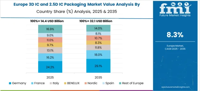
The 3D IC and 2.5D IC packaging market in France is projected to expand at a CAGR of 9.5% from 2025 to 2035, supported by research-driven initiatives and government incentives for semiconductor R&D. France plays a crucial role in European semiconductor strategy, focusing on automotive electronics, aerospace, and industrial automation where reliability and miniaturization are vital. Adoption is reinforced by partnerships with major European chipmakers and institutes focusing on heterogeneous integration. Pilot projects in renewable energy and edge computing reinforce demand for advanced packaging solutions. France is developing a quality-driven market, where innovation pipelines and government-funded programs create sustainable momentum despite its smaller production base.
The 3D IC and 2.5D IC packaging market in the UK is anticipated to grow at a CAGR of 8.6% between 2025 and 2035, with strong emphasis on design leadership, R&D partnerships, and pilot-scale semiconductor projects. The UK focuses on advanced packaging for AI, defense, and quantum computing applications, with universities and research institutions contributing to cutting-edge design. Though large-scale fabrication is limited, international partnerships allow access to advanced manufacturing capacity. Startups in chip design are adopting chiplet-based architectures, ensuring steady demand for 2.5D interposers and 3D stacking. The UK’s role will be defined more by design innovation and niche application strength than by mass production.
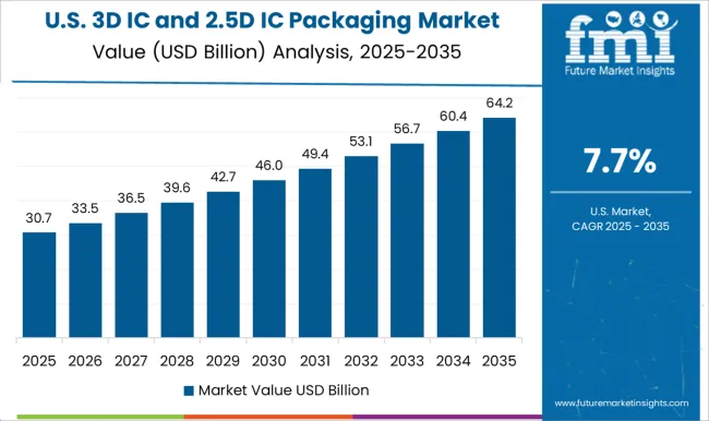
The 3D IC and 2.5D IC packaging market in the USA is projected to grow at a CAGR of 7.7% from 2025 to 2035, with growth anchored in defense electronics, high-performance computing, and hyperscale data centers. USA semiconductor firms are at the forefront of developing chiplet architectures, with strong integration into AI and cloud ecosystems. Government-backed programs such as the CHIPS Act are funding advanced packaging R&D and manufacturing initiatives. Automotive and aerospace sectors also drive adoption, requiring reliable, thermally efficient chip packages for mission-critical applications. While growth is steadier compared to Asia, the USA maintains leadership in innovation, IP ownership, and early commercialization of advanced 3D packaging technologies.
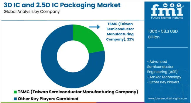
Competition in the 3D IC and 2.5D IC packaging market is defined by integration density, advanced interconnect solutions, and efficiency in high-performance computing applications. TSMC (Taiwan Semiconductor Manufacturing Company) leads with cutting-edge wafer-level packaging and through-silicon-via (TSV) technologies, dominating global demand through strong foundry capabilities and partnerships with leading fabless firms. Samsung Electronics and Intel Corporation compete closely by leveraging their advanced node capabilities and in-house design-to-packaging integration, focusing on data centers, AI processors, and consumer electronics. Amkor Technology and Advanced Semiconductor Engineering (ASE) differentiate as outsourced semiconductor assembly and test (OSAT) leaders, offering scalable 2.5D and 3D integration platforms that support global fabless chipmakers.
Broadcom, Xilinx, and Texas Instruments emphasize customized solutions for networking, FPGAs, and analog-intensive applications, reinforcing the role of packaging in enhancing device performance. Companies like JCET, SPIL, Powertech Technology Inc. (PTI), and ChipMOS Technologies serve as essential global OSAT players, providing cost-competitive packaging with regional strengths in Asia. Japanese firms Mitsubishi Electric Corporation and Toshiba Corporation focus on automotive, industrial, and energy applications where reliability and thermal management are critical, while United Microelectronics Corporation (UMC) contributes by combining foundry and packaging capabilities for select markets. Strategic initiatives across these companies highlight collaborations with equipment manufacturers, ecosystem partnerships, and heavy investment in R&D to improve yield rates and manage costs in TSV and interposer-based technologies. Product documentation across the industry highlights features such as interposer thickness, TSV density, thermal dissipation efficiency, and compatibility with logic-memory integration. Brochures emphasize performance metrics, power consumption reduction, and system-level optimization.
Competitive strategies emphasize differentiation through heterogeneous integration, ecosystem alignment with AI and 5G markets, and co-development with fabless and systems companies. The market is marked by a blend of foundry dominance, OSAT scale, and specialized providers carving niches in automotive, networking, and FPGA-driven demand.
| Item | Value |
|---|---|
| Quantitative Units | USD 58.3 Billion |
| Technology | 3D TSV, 3D wafer-level chip-scale packaging, and 2.5D |
| Application | Logic, Memory, Imaging & optoelectronics, MEMS/Sensors, LED, and Others |
| End Use | Consumer electronics, Telecommunication, Automotive, Military & aerospace, Medical devices, Smart technologies, and Others |
| Regions Covered | North America, Europe, Asia-Pacific, Latin America, Middle East & Africa |
| Country Covered | United States, Canada, Germany, France, United Kingdom, China, Japan, India, Brazil, South Africa |
| Key Companies Profiled | TSMC (Taiwan Semiconductor Manufacturing Company), Advanced Semiconductor Engineering (ASE), Amkor Technology, Broadcom, ChipMOS Technologies Inc, Intel Corporation, Jiangsu Changjiang Electronics Technology (JCET), Mitsubishi Electric Corporation, Powertech Technology Inc. (PTI), Samsung Electronics, Siliconware Precision Industries (SPIL), Texas Instrument, Toshiba Corporation, United Microelectronics Corporation (UMC), and Xilinx Inc. |
| Additional Attributes | Dollar sales, share, competitive benchmarking, regional adoption patterns, OSAT vs foundry contributions, yield challenges, supply chain risks, government incentives, customer demand in AI/data centers/automotive, and long-term adoption forecasts. |
The global 3D IC and 2.5D IC packaging market is estimated to be valued at USD 58.3 billion in 2025.
The market size for the 3D IC and 2.5D IC packaging market is projected to reach USD 138.0 billion by 2035.
The 3D IC and 2.5D IC packaging market is expected to grow at a 9.0% CAGR between 2025 and 2035.
The key product types in 3D IC and 2.5D IC packaging market are 3d tsv, 3d wafer-level chip-scale packaging and 2.5d.
In terms of application, logic segment to command 45.9% share in the 3D IC and 2.5D IC packaging market in 2025.

Full Research Suite comprises of:
Market outlook & trends analysis
Interviews & case studies
Strategic recommendations
Vendor profiles & capabilities analysis
5-year forecasts
8 regions and 60+ country-level data splits
Market segment data splits
12 months of continuous data updates
DELIVERED AS:
PDF EXCEL ONLINE
3D Printing Industry Analysis in Middle East Size and Share Forecast Outlook 2025 to 2035
3D Printed Dental Brace Market Size and Share Forecast Outlook 2025 to 2035
3D Reverse Engineering Software Market Forecast and Outlook 2025 to 2035
3D Printing Metal Market Size and Share Forecast Outlook 2025 to 2035
3D Bioprinted Organ Transplants Market Size and Share Forecast Outlook 2025 to 2035
3D Audio Market Size and Share Forecast Outlook 2025 to 2035
3D Printed Maxillofacial Implants Market Size and Share Forecast Outlook 2025 to 2035
3D-Printed Personalized Masks Market Size and Share Forecast Outlook 2025 to 2035
3D Printing Market Size and Share Forecast Outlook 2025 to 2035
3D Printed Clear Dental Aligners Market Size and Share Forecast Outlook 2025 to 2035
3d-Printed Skincare Market Analysis - Size and Share Forecast Outlook 2025 to 2035
3D Display Market Size and Share Forecast Outlook 2025 to 2035
3D Neuroscience Market Size and Share Forecast Outlook 2025 to 2035
3D Glasses Market Size and Share Forecast Outlook 2025 to 2035
3D Printing in Automotive Market Size and Share Forecast Outlook 2025 to 2035
3D Printing In Construction Market Size and Share Forecast Outlook 2025 to 2035
3D Bioprinted Human Tissue Market Analysis - Size, Share, and Forecast 2025 to 2035
3D Laser Scanner Market Growth - Trends & Forecast 2025 to 2035
3D Knitting Machines Market Size and Share Forecast Outlook 2025 to 2035
3D Scanning Market Size and Share Forecast Outlook 2025 to 2035

Thank you!
You will receive an email from our Business Development Manager. Please be sure to check your SPAM/JUNK folder too.
Chat With
MaRIA