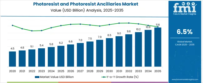
The photoresist and photoresist ancillaries market is estimated to be valued at USD 6.2 billion in 2025 and is projected to reach USD 11.6 billion by 2035, registering a compound annual growth rate (CAGR) of 6.5% over the forecast period.
The trajectory shows a steady climb, with values reaching 7.0 billion in 2027 and 7.9 billion in 2029, pointing to growing adoption across semiconductor fabrication and microelectronics. Analysts highlight that the CAGR curve indicates consistent expansion rather than aggressive spikes, shaped by increasing wafer production and lithography upgrades. The curve is considered a reflection of stable end-use integration where performance reliability and material innovation play a crucial role in shaping long-term demand.
By 2030, values are expected to touch 8.5 billion, followed by 9.6 billion in 2032 and 10.9 billion in 2034, closing at 11.6 billion in 2035. This compound annual progression underscores strong ties with chip manufacturing and high-resolution display technologies, where precision coating and etching materials are critical. Experts suggest the CAGR curve validates photoresist as a strategic enabler in semiconductor ecosystems, reinforcing supply chain depth and material performance. The growth outlook is perceived as reliable, with the market positioned to capture opportunities created by advanced electronic architectures and expanding lithography equipment deployment worldwide.
| Metric | Value |
|---|---|
| Photoresist and Photoresist Ancillaries Market Estimated Value in (2025 E) | USD 6.2 billion |
| Photoresist and Photoresist Ancillaries Market Forecast Value in (2035 F) | USD 11.6 billion |
| Forecast CAGR (2025 to 2035) | 6.5% |
The photoresist and photoresist ancillaries segment is estimated to contribute nearly 14% of the semiconductor materials market, about 16% of the electronic chemicals market, close to 22% of the photolithography materials market, nearly 12% of the advanced packaging materials market, and around 15% of the microelectronics materials market. Collectively, this represents an aggregated share of approximately 79% across its parent categories. Such a proportion highlights the essential role of photoresists and ancillaries in enabling circuit patterning, miniaturization, and high-precision manufacturing processes in semiconductors. Their relevance has been established in ensuring accuracy during wafer fabrication, where even marginal improvements translate into higher yield and performance gains.
Industry specialists often view this segment as a strategic pillar within the semiconductor ecosystem, since without reliable photoresists, lithography cannot deliver the scaling and complexity demanded by advanced chips. The market’s value has been reinforced by ongoing transitions to finer nodes, with demand growing in memory, logic devices, and advanced packaging formats. Their influence is seen not only in semiconductor fabs but also in upstream supply chains that rely on consistent material performance and tight quality control. As such, photoresists and ancillaries are not regarded as interchangeable commodities but as high-value enablers that underpin the competitive edge of leading semiconductor companies, cementing their position as an indispensable part of the broader electronics materials landscape.
The photoresist and photoresist ancillaries market is experiencing steady expansion, fueled by the rapid evolution of semiconductor manufacturing and the growing complexity of integrated circuit designs. Industry announcements and technology roadmaps from leading semiconductor companies have emphasized the critical role of advanced photoresists in enabling smaller, faster, and more power-efficient chips.
The shift toward extreme ultraviolet (EUV) lithography and multi-patterning techniques has created sustained demand for high-performance photoresist materials with enhanced resolution and sensitivity. Additionally, growth in consumer electronics, automotive electronics, and industrial IoT devices has driven higher wafer fabrication volumes, directly boosting market consumption.
Investments in new fabrication facilities, particularly in Asia-Pacific, have strengthened regional supply chains and increased the adoption of advanced ancillaries such as anti-reflective coatings and developers. Looking ahead, the market is expected to benefit from ongoing R&D collaborations aimed at developing next-generation photoresists compatible with emerging lithography technologies and advanced node production, ensuring continued relevance in the rapidly progressing semiconductor industry.
The photoresist and photoresist ancillaries market is segmented by product, application, and geographic regions. By product, photoresist and photoresist ancillaries market is divided into photoresist, G-line and I-line, KrF, ArF Dry, ArF Immersion, photoresist ancillaries, antireflective coatings, photoresist developers, edge bead removers, and others. In terms of application, photoresist and photoresist ancillaries market is classified into semiconductors & integrated circuits, printed circuit boards, and others. Regionally, the photoresist and photoresist ancillaries industry is classified into North America, Latin America, Western Europe, Eastern Europe, Balkan & Baltic Countries, Russia & Belarus, Central Asia, East Asia, South Asia & Pacific, and the Middle East & Africa.
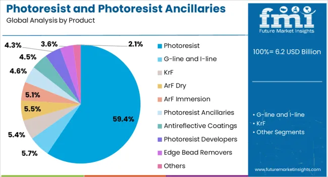
The photoresist segment is projected to hold 59.40% of the market revenue in 2025, securing its lead as the primary material type in lithographic processes. This dominance has been driven by its essential function in transferring intricate circuit patterns onto semiconductor wafers with precision and efficiency. Advances in lithography technologies, including EUV and deep ultraviolet (DUV), have increased the performance requirements for photoresists, prompting material innovations that improve resolution, sensitivity, and etch resistance.
Semiconductor fabrication plants have relied heavily on optimized photoresist formulations to achieve consistent yields at advanced technology nodes, ensuring competitiveness in a market driven by miniaturization trends. Furthermore, the broad compatibility of photoresists with various substrate materials and lithography systems has reinforced their widespread adoption across global foundries. Continuous collaboration between material suppliers and semiconductor manufacturers is expected to sustain the segment’s growth, as next-generation chip designs demand even more sophisticated resist performance.
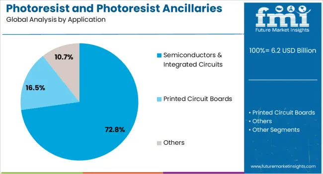
The semiconductors & integrated circuits segment is projected to account for 72.80% of the market revenue in 2025, maintaining its position as the dominant application area. Growth in this segment has been supported by the escalating demand for high-performance computing, mobile devices, automotive electronics, and AI-driven technologies, all of which require advanced semiconductor components.
Photoresists and related ancillaries are indispensable in defining the micro- and nanoscale features that underpin modern integrated circuit performance. The proliferation of connected devices and expansion of 5G networks have increased chip production volumes, amplifying the consumption of photoresist materials in wafer fabrication.
Additionally, significant capital investments in semiconductor fabrication facilities by leading foundries and integrated device manufacturers have reinforced long-term demand for lithographic materials. As the semiconductor industry moves toward more complex architectures and smaller geometries, the application segment is expected to maintain its growth trajectory, supported by sustained technological innovation and global capacity expansion.
The photoresist and photoresist ancillaries market is projected to advance with rising semiconductor production, expanding display manufacturing, and growing demand for microelectronics. Demand is stimulated by lithography processes in integrated circuits and flat-panel displays. Opportunities are opening with the surge in advanced chip fabrication, OLED panels, and MEMS devices. Trends highlight a shift toward extreme ultraviolet (EUV) resists, improved ancillary chemicals, and region-specific supply chain integration. Challenges such as high R&D costs, raw material dependencies, and regulatory complexities continue to shape the trajectory of this specialized chemical domain.
Demand for photoresist and its ancillaries has been reinforced by the expanding semiconductor and display industries. Lithography has been a critical step in fabricating integrated circuits, where photoresists define circuit patterns with precision. Growing production of OLEDs, LCDs, and MEMS devices has also strengthened the requirement for advanced resists and supporting ancillaries. Opinions suggest that the market’s strongest demand drivers lie in consumer electronics and automotive sectors, where microelectronics adoption has accelerated. Rapid digital transformation has pushed manufacturers to scale up production capacity, ensuring consistent supply of these essential materials. Demand has also been amplified by the rollout of 5G infrastructure and advanced packaging needs. With miniaturization of electronics progressing, demand for photoresist formulations and ancillaries capable of delivering higher resolution and stability is set to remain a decisive growth factor.
Opportunities in the photoresist and photoresist ancillaries market are being created by the transition to advanced lithography technologies such as EUV. Semiconductor manufacturers are increasingly adopting EUV photoresists to achieve smaller node sizes and higher integration levels. Ancillaries such as anti-reflective coatings and developers are being optimized to complement EUV systems, unlocking new revenue potential for suppliers. Opinions indicate that the most promising opportunities lie in advanced chip packaging, where resists enable finer interconnects for high-performance computing and AI-driven devices. Growth in OLED and quantum dot displays is further broadening opportunities for innovative resist chemistries. Emerging economies building semiconductor fabs are expected to provide new avenues for suppliers of resists and ancillaries. These developments suggest that companies focusing on high-resolution, defect-minimized materials can secure strong competitive positioning in a rapidly evolving ecosystem.
Trends in the photoresist and ancillaries market revolve around innovation in formulations, supply chain localization, and collaboration between chemical firms and chipmakers. The shift toward EUV has created demand for new resist chemistries capable of addressing line edge roughness and defectivity. Ancillary chemicals are trending toward low-volatility, environmentally compliant formulations that support high yields. Opinions suggest that another trend lies in vertical integration, as chipmakers pursue direct partnerships with chemical firms to secure long-term supply stability. Regionalization of supply chains has been observed, with Asia Pacific gaining prominence in both consumption and production. Investment in R&D pipelines for chemically amplified resists and underlayer coatings is also trending upward. Collectively, these shifts represent a market trajectory that is less commoditized and increasingly reliant on innovation, partnerships, and localized ecosystems for growth.
Challenges facing the photoresist and photoresist ancillaries market include high R&D costs, raw material dependencies, and stringent compliance requirements. Developing resists compatible with EUV and advanced lithography nodes requires significant investment, which only a limited number of suppliers can sustain. Raw material shortages and reliance on specialized chemical intermediates create vulnerabilities in supply continuity. Opinions highlight that compliance with regional chemical safety regulations adds further complexity, delaying commercialization timelines. Smaller firms struggle to compete due to the high entry barriers, leaving the market concentrated among a few major players. Cost pressures from chipmakers demanding reliable yet affordable materials have amplified the challenge. This structural imbalance underscores why only suppliers with strong financial and technical resources are able to compete effectively, while others risk being marginalized in an industry defined by innovation and scale.
| Country | CAGR |
|---|---|
| China | 8.8% |
| India | 8.1% |
| Germany | 7.5% |
| France | 6.8% |
| U.K. | 6.2% |
| U.S. | 5.5% |
| Brazil | 4.9% |
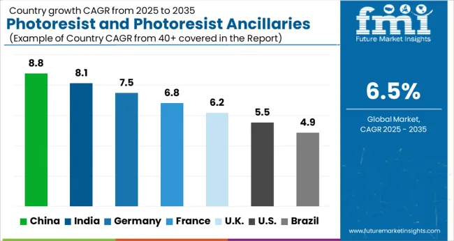
The global photoresist and photoresist ancillaries market is projected to expand at a CAGR of 6.5% between 2025 and 2035. China is forecast to lead at 8.8%, followed by India at 8.1% and Germany at 7.5%. The United Kingdom is expected to register 6.2%, while the United States posts 5.5%. Growth is supported by expanding semiconductor production, rising flat panel display demand, and broader use in printed circuit boards. Asian markets grow faster due to strong government support and domestic fabrication initiatives, while Europe leverages demand from automotive and industrial electronics. The U.S. market, though slower, remains significant due to niche applications in defense, aerospace, and advanced packaging technologies. This report includes insights on 40+ countries; the top markets are shown here for reference.
The photoresist and photoresist ancillaries market in China is projected to grow at a CAGR of 8.8%. Strong national focus on semiconductor independence and consumer electronics manufacturing drives expansion. Investment in fabs, flat panel display plants, and printed circuit board facilities creates large scale demand for advanced resists and ancillary products. Strategic partnerships with international suppliers ensure access to technology while encouraging domestic development of formulations. Rapid urban consumption patterns, coupled with demand for automotive electronics, reinforce long term momentum. The government’s role in financing and incentivizing infrastructure projects guarantees sustained adoption. China’s position as both a production hub and end market consolidates its leadership in the global landscape.
The photoresist and photoresist ancillaries market in India is expected to grow at a CAGR of 8.1%. Expansion is propelled by rising electronics manufacturing, growth of printed circuit board facilities, and government programs supporting domestic semiconductor fabrication. India’s electronics parks and Make in India initiatives provide incentives for local production, reducing import reliance. Consumer electronics, LED manufacturing, and automotive electronics further reinforce demand for high performance resists and ancillaries. Collaboration with international players ensures technology transfer, while defense and aerospace projects expand long term adoption. Increasing private and public investment signals a strategic pivot toward semiconductor self sufficiency, strengthening India’s presence in the global photoresist value chain.
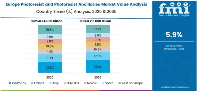
The photoresist and photoresist ancillaries market in Germany is projected to grow at a CAGR of 7.5%. Demand is anchored by the country’s strong automotive electronics, industrial automation, and semiconductor equipment industries. German manufacturers emphasize precision and high reliability, driving adoption of specialized resists for MEMS, sensors, and control systems. Partnerships between local chemical producers and equipment firms foster innovation tailored to industrial needs. Circular demand from advanced manufacturing and Industry 4.0 initiatives increases integration of high resolution lithography. Germany’s role as a European semiconductor and electronics hub ensures a balanced growth trajectory, with steady investment supporting both domestic use and export oriented applications.
The photoresist and photoresist ancillaries market in the UK is forecast to grow at a CAGR of 6.2%. Growth is driven by applications in printed circuit boards, optoelectronics, and specialty semiconductor development. The UK’s ecosystem emphasizes research collaborations between universities, startups, and international suppliers to advance high performance formulations. Adoption is concentrated in niche markets such as defense, healthcare electronics, and specialty design houses rather than large scale fabs. Public procurement and investment in defense technology ensure recurring demand, while private firms focus on premium and high precision applications. Though moderate in pace, the UK’s strategy of niche specialization helps preserve competitiveness in the broader global value chain.
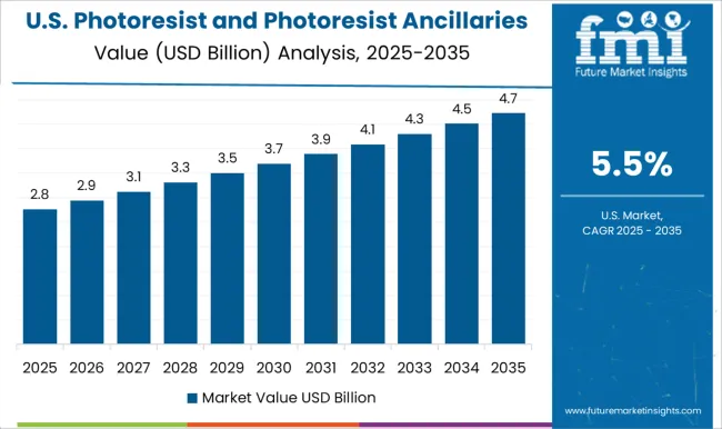
The photoresist and photoresist ancillaries market in the US is expected to expand at a CAGR of 5.5%. The market is shaped by established semiconductor infrastructure with slower expansion compared to Asia, yet niche adoption in aerospace, defense, and advanced packaging remains strong. U.S. manufacturers emphasize reliability, purity, and compliance, supporting applications that demand high performance. Research into next generation lithography, including EUV and advanced resists, maintains technological leadership despite limited volume growth. Federal funding and private sector collaboration provide momentum for innovation pipelines, while imports supplement mass scale needs. Growth is steady, underscored by specialization and strategic positioning in global semiconductor supply chains.
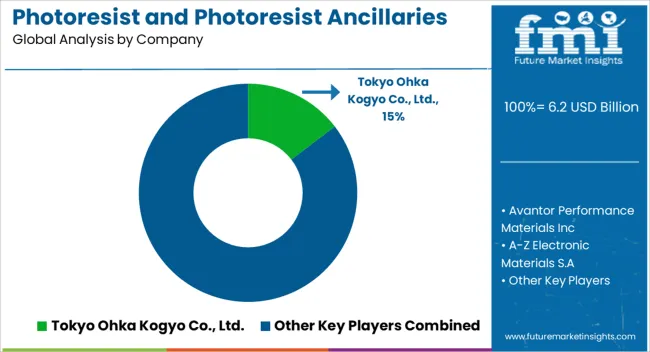
Competition in photoresists and ancillaries has been centered on how clearly companies position chemistry portfolios through brochures and selector guides. Tokyo Ohka Kogyo, JSR Corporation, and Shin-Etsu Chemical present detailed product sheets that showcase advanced ArF, KrF, and EUV resists, emphasizing line edge roughness, etch resistance, and critical dimension control. FUJIFILM Electronic Materials highlights a wide catalogue that frames developers, strippers, and topcoats alongside resists, with brochures stressing process integration. Sumitomo Chemical and LG Chem communicate competitiveness through brochures that stress polymer design, defect reduction, and integration with advanced nodes.
Dow Chemical and DuPont underline long standing credibility by publishing selector guides that highlight compatibility across lithography generations. Eternal Materials and Kolon Industries position brochures around cost effective KrF resists and ancillary chemistries for regional fabs. The competitive landscape is shaped by how technical brochures condense complex chemistry into repeatable performance promises. Strategies focus on credibility through documentation and application notes. Avantor and A-Z Electronic Materials present brochures that emphasize purity standards, contamination control, and global supply capabilities. HTP HiTech Photopolymere and Asahi Kasei differentiate with brochures that highlight niche formulations for packaging, MEMS, and display panels. Hitachi Chemical stresses ancillaries and underlayers, issuing brochures that call out anti reflective coatings and adhesion promoters.
Product literature is consistently dense with graphs, defectivity data, and application windows, allowing buyers to compare across suppliers. Success is less about slogans and more about how brochures demonstrate resolution, sensitivity, and etch selectivity at advanced nodes. Competition is decided when a supplier’s documents show proven performance in fab trials, quantified yield improvements, and compatibility with lithography tools. In this market, the product brochure becomes both the sales pitch and the technical evidence, making it the decisive battleground for supplier choice.
| Item | Value |
|---|---|
| Quantitative Units | USD 6.2 billion |
| Product | Photoresist, G-line and I-line, KrF, ArF Dry, ArF Immersion, Photoresist Ancillaries, Antireflective Coatings, Photoresist Developers, Edge Bead Removers, and Others |
| Application | Semiconductors & Integrated Circuits, Printed Circuit Boards, and Others |
| Regions Covered | North America, Europe, Asia-Pacific, Latin America, Middle East & Africa |
| Country Covered | United States, Canada, Germany, France, United Kingdom, China, Japan, India, Brazil, South Africa |
| Key Companies Profiled | Tokyo Ohka Kogyo Co., Ltd., Avantor Performance Materials Inc, A-Z Electronic Materials S.A, The Dow Chemicals Company, E. I. du Pont de Nemours and Company (DuPont), FUJIFILM Electronic Materials Co., Ltd., JSR Corporation, Shin-Etsu Chemical Co., Ltd., Sumitomo Chemical Co., Ltd., LG Chem, Ltd., Eternal Materials Co.,Ltd., HTP HiTech Photopolymere AG, Kolon Industries, Asahi Kasei Corporation, and Hitachi Chemical Co., Ltd. |
| Additional Attributes | Dollar sales by product type (ArF immersion, ArF dry, KrF, g-line & i-line), Dollar sales by ancillaries (anti-reflective coatings, developers, removers, edge bead removers), Trends in semiconductor lithography and EUV adoption, Role of photoresists in advanced IC manufacturing and packaging, Growth of demand in memory and logic device production, Regional manufacturing concentration in Asia Pacific, North America, and Europe. |
The global photoresist and photoresist ancillaries market is estimated to be valued at USD 6.2 billion in 2025.
The market size for the photoresist and photoresist ancillaries market is projected to reach USD 11.6 billion by 2035.
The photoresist and photoresist ancillaries market is expected to grow at a 6.5% CAGR between 2025 and 2035.
The key product types in photoresist and photoresist ancillaries market are photoresist, g-line and i-line, krf, arf dry, arf immersion, photoresist ancillaries, antireflective coatings, photoresist developers, edge bead removers and others.
In terms of application, semiconductors & integrated circuits segment to command 72.8% share in the photoresist and photoresist ancillaries market in 2025.





Full Research Suite comprises of:
Market outlook & trends analysis
Interviews & case studies
Strategic recommendations
Vendor profiles & capabilities analysis
5-year forecasts
8 regions and 60+ country-level data splits
Market segment data splits
12 months of continuous data updates
DELIVERED AS:
PDF EXCEL ONLINE
Photoresist Chemical Market Forecast and Outlook 2025 to 2035
Photoresist Electronic Chemical Market Size and Share Forecast Outlook 2025 to 2035
Photoresist Stripper Market Analysis - Size, Share, and Forecast 2025 to 2035
Android Automotive OS (AAOS) Market Size and Share Forecast Outlook 2025 to 2035
Anderson Cascade Impactor Market Size and Share Forecast Outlook 2025 to 2035
Andersen-Tawil Syndrome Treatment Market Trends - Growth & Future Prospects 2025 to 2035
Andro Supplements Market
Hand Towel Automatic Folding Machine Market Size and Share Forecast Outlook 2025 to 2035
Handheld Ultrasound Scanner Market Size and Share Forecast Outlook 2025 to 2035
Handheld Tagging Gun Market Forecast and Outlook 2025 to 2035
Handheld Imaging Systems Market Size and Share Forecast Outlook 2025 to 2035
Sandwich Panel System Market Size and Share Forecast Outlook 2025 to 2035
Hand Tools Market Size and Share Forecast Outlook 2025 to 2035
Land Survey Equipment Market Size and Share Forecast Outlook 2025 to 2035
Handloom Product Market Size and Share Forecast Outlook 2025 to 2035
Band File Sander Belts Market Size and Share Forecast Outlook 2025 to 2035
Handheld XRF Analyzers Market Size and Share Forecast Outlook 2025 to 2035
Sand Abrasion Tester Market Size and Share Forecast Outlook 2025 to 2035
Sand Testing Equipments Market Size and Share Forecast Outlook 2025 to 2035
Landscape Lighting Market Size and Share Forecast Outlook 2025 to 2035

Thank you!
You will receive an email from our Business Development Manager. Please be sure to check your SPAM/JUNK folder too.
Chat With
MaRIA