- Market Size (2026)
- USD 24.5 Mn
- Forecast (2036)
- USD 219.2 Mn
- CAGR (2026 to 2036)
- 24.5%
How big is Skyrmion Racetrack Memories Market in 2026?
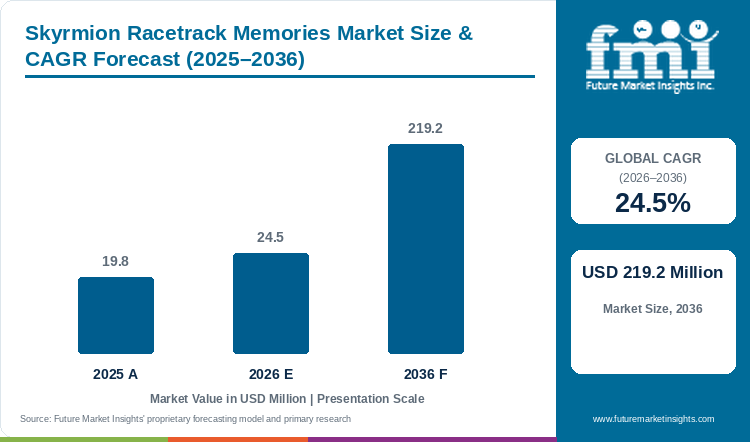
Valued at USD 19.8 million during 2025, global skyrmion racetrack memories revenue reaches an estimated USD 24.5 million in 2026 before climbing to a projected USD 219.2 million by 2036 on a 24.5% CAGR.
Antisymmetric Dzyaloshinskii-Moriya exchange interactions at heavy-metal interfaces stabilize sub-10-nanometer chiral spin whirls along magnetic nanowires so solid-state shift registers move bit domains without mechanical read heads. Orbital avionics engineers and hyperscale AI hardware architects specify these topological memory tracks because conventional charge-based SRAM and flash cells suffer single-event upset bit flips and high static leakage currents. After registering USD 19.8 million in 2025, worldwide skyrmion racetrack memories valuation reaches an estimated USD 24.5 million for 2026 and is forecast to hit USD 219.2 million by 2036 through a 24.5% CAGR that yields USD 194.7 million in new revenue. In August 2025, U.S. NIST physicists demonstrated that neuromorphic hardware networks can learn autonomously on-chip while slashing training energy [1]. Synthetic Antiferromagnetic (SAF) CoFeB/Pt/Ir Heavy-Metal Tracks are slated to represent 58.6% of 2026 stack demand alongside multi-cathode sputtering deposition systems inside 300-millimeter semiconductor fabs.
Key Market Trends & Insights
- By chiral magnetic multilayer stack: Synthetic Antiferromagnetic (SAF) CoFeB/Pt/Ir Heavy-Metal Tracks are projected to capture 58.6% of 2026 stack expenditure because bilinear ruthenium-iridium spacer coupling suppresses skyrmion Hall edge annihilation.
- By nucleation & readout mechanism: Spin-Orbit Torque (SOT) Current-Driven + MTJ Tunnel Readout is expected to command 66.4% of 2026 readout turnover since perpendicular magnetic tunnel junctions deliver over 150% tunnel magnetoresistance ratios on standard CMOS sense amplifiers.
- By target computing application: Radiation-Hardened Space & Defense Non-Volatile Cache is anticipated to secure 44.2% of 2026 application spending as geostationary satellite payloads replace heavy radiation-shielded SRAM modules with topologically protected nanowire buffers.
- By package substrate size & process node: 55x55 mm to 75x75 mm FCBGA High-Pin-Count substrates are forecast to hold 63.4% of 2026 packaging volume while 4nm / 5nm FinFET Low-Power SerDes Node wafers account for 66.8% of node revenue.
Regional Highlights
- Top national expansion pace: South Korea is projected to pace the six major semiconductor countries at a 26.3% compound annual clip through 2036 on the back of foundry back-end-of-line spintronic memory pilot lines in Gyeonggi Province.
- Secondary Asian and European momentum: Taiwanese wafer foundries are forecast to advance by 25.7% annually and French defense spintronics labs are expected to follow at 25.2% through 2036.
- Mature foundry and equipment baselines: United States defense memory fabs are estimated to expand by 24.1% yearly ahead of Japanese precision magnetic tooling suppliers (23.8%) and German vacuum PVD equipment makers (23.5%).
Market Size & Forecast
Table 1: Market Size and Forecast for the Skyrmion Racetrack Memories Market (USD million and CAGR percentage), 2025 to 2036
| Metric | Value |
|---|---|
| 2025 Market Size | USD 19.8 million |
| Estimated Market Size in 2026 | USD 24.5 million |
| Projected Market Size by 2036 | USD 219.2 million |
| CAGR, 2026 to 2036 | 24.5% |
| Added Revenue, 2026 to 2036 | USD 194.7 million |
Sovereign microelectronics funding programs across North America and East Asia are accelerating the transition of chiral domain-wall shift registers from university cleanrooms into 300-millimeter CMOS back-end-of-line pilot lines. In May 2026, U.S. CHIPS Research and Development officials announced USD 2.0 billion in letters of intent with nine semiconductor companies to accelerate domestic topological and spin microelectronics [2]. Consequently, defense prime contractors and foundry consortia are pairing chiral nanowire shift registers with next-generation non-volatile memory arrays to eliminate off-chip DRAM bus latency. Device vendors that maintain sub-angstrom platinum and iridium interface roughness across eight-inch and twelve-inch wafers secure multi-year qualification contracts with satellite avionics integrators.
Wafer Shuttle Volume and Racetrack Bit-Density Sizing
Table 2: Wafer Shuttle Volume and Racetrack Bit-Density Indicators for the Skyrmion Racetrack Memories Market (USD million, wafer equivalents, and gigabits per square millimeter), mixed historical and forecast years from 2025 to 2036
| Metric | 2025 | 2026 | 2036 |
|---|---|---|---|
| Market size (USD million) | 19.8 | 24.5 | 219.2 |
| Annual 300mm-equivalent spintronic wafer shuttles (wafers) | 1,420 to 1,650 | 1,750 to 2,050 | 16,800 to 19,400 |
| Effective skyrmion bit pitch along nanowire tracks (nm) | 18 to 25 | 14 to 20 | 5 to 8 |
| Realized foundry shuttle & die value per wafer (USD thousand) | 12.0 to 13.9 | 12.0 to 14.0 | 11.3 to 13.0 |
Operational note: Wafer shuttle volumes reflect 200-millimeter and 300-millimeter multi-project wafer runs and radiation-hardened defense lot shipments carrying chiral magnetic multilayer stacks between 12 and 40 repeats.
Scaling chiral nanowire bit density requires atomic-layer control over interfacial Dzyaloshinskii-Moriya exchange constants so thermal fluctuations do not prematurely annihilate skyrmion lattice domains during standby retention. In December 2025, condensed-matter authors in Physical Review B demonstrated hybrid magnetic-superconducting nanostructures that stabilize nanoscale skyrmion states at zero external magnetic field [3]. Foundry process engineers combine these pinning geometries with magnetron sputtering vacuum clusters to fabricate uniform single-skyrmion shift registers.
Foundry Line Allocation & Avionics Program Spending
Table 3: Foundry Line Allocation and Program Spending Indicators for the Skyrmion Racetrack Memories Market (USD and facility metrics), mixed historical and forecast years from 2025 to 2036
| Metric | 2025 | 2026 | 2036 |
|---|---|---|---|
| Active spintronic BEOL & defense foundry lines worldwide | 18 | 22 | 64 |
| Average annual skyrmion memory spend per active line (USD million) | 1.10 | 1.11 | 3.43 |
| Spend per qualified aerospace & AI compute program (USD thousand) | 310 to 360 | 345 to 410 | 920 to 1,150 |
| Average SOT current density for 100 m/s domain motion (MA/cm²) | 18 to 24 | 15 to 20 | 6 to 9 |
Table 4: Segment Revenue & Foundry Allocation Benchmarks for the Skyrmion Racetrack Memories Market (USD million and percentages), mixed reporting years from 2025 to 2026
| Benchmark Indicator | Reported / Modeled Value | Institutional Reference Basis |
|---|---|---|
| Market size, 2026 | USD 24.5 million | Report value |
| SAF CoFeB/Pt/Ir heavy-metal track revenue, 2026 | USD 14.4 million | 58.6% stack share |
| SOT current-driven + MTJ readout revenue, 2026 | USD 16.3 million | 66.4% readout share |
| Radiation-hardened space & defense cache revenue, 2026 | USD 10.8 million | 44.2% application share |
Defense microelectronics fabricators and neuromorphic chip designers allocate dedicated physical vapor deposition chambers to chiral multilayer stacks so heavy-metal cross-contamination never degrades standard CMOS logic yields. Integrating spintronic nanowire shift registers directly above radiation-hardened electronics substrates allows orbital flight computers to survive proton belt transit without triple-modular redundancy penalties. As 4nm and 5nm FinFET logic nodes tighten interconnect pitch, high-pin-count flip-chip ball grid arrays remain essential for routing nanosecond spin-orbit torque drive pulses.
Analyst Perspective
"Synthetic antiferromagnetic CoFeB/Pt/Ir tracks eliminate the skyrmion Hall effect and make sub-10-nanometer nanowire shift registers manufacturable on 300-millimeter CMOS wafers. Foundry engineers must still reduce spin-orbit torque nucleation current densities below ten mega-amperes per square centimeter to prevent electromigration in FinFET via pillars."
- Sudip Saha, Co-founder, Future Market Insights.
How is the skyrmion racetrack memories market segmented?
The skyrmion racetrack memories market is segmented by chiral magnetic multilayer stack, nucleation & readout mechanism, target computing application, package substrate size, process node, and region. In 2026, Synthetic Antiferromagnetic (SAF) CoFeB/Pt/Ir Heavy-Metal Tracks is projected at 58.6%, Spin-Orbit Torque (SOT) Current-Driven + MTJ Tunnel Readout at 66.4%, Radiation-Hardened Space & Defense Non-Volatile Cache at 44.2%, 55x55 mm to 75x75 mm FCBGA High-Pin-Count at 63.4%, and 4nm / 5nm FinFET Low-Power SerDes Node at 66.8%.
By chiral magnetic multilayer stack: Synthetic Antiferromagnetic (SAF) CoFeB/Pt/Ir Heavy-Metal Tracks, Ferrimagnetic GdFeCo Zero-Skyrmion-Hall-Angle Nanowires, and 2D Van der Waals Ferromagnet (Fe3GeTe2) Heterostructures.
By nucleation & readout mechanism: Spin-Orbit Torque (SOT) Current-Driven + MTJ Tunnel Readout, Voltage-Controlled Magnetic Anisotropy (VCMA) Gated Tracks, and Topological Hall-Effect & Optical Kerr Readout Arrays.
By target computing application: Radiation-Hardened Space & Defense Non-Volatile Cache, Stochastic & Brownian Reservoir Neuromorphic Accelerators, and Ultra-Dense Last-Level CPU/GPU Working Memory Replacement.
By package substrate size: 55x55 mm to 75x75 mm FCBGA High-Pin-Count, <55x55 mm Compact Edge Switch Package, and Wafer-Level Known-Good-Die (KGD) Cryogenic & 2.5D Interposers.
By process node: 4nm / 5nm FinFET Low-Power SerDes Node, 3nm Advanced SerDes Node, and 14nm to 28nm Rad-Hard CMOS Back-End-of-Line (BEOL) Node.
Why Do Synthetic Antiferromagnetic CoFeB/Pt/Ir Heavy-Metal Tracks Dominate Chiral Multilayer Stack Selection?
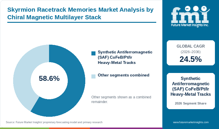
Synthetic Antiferromagnetic (SAF) CoFeB/Pt/Ir Heavy-Metal Tracks hold 58.6% of chiral magnetic multilayer stack demand in 2026, supported by zero-deflection domain velocity.
Table 5: Chiral Magnetic Multilayer Stack Share for the Skyrmion Racetrack Memories Market (percentage share), 2026
| Chiral Magnetic Multilayer Stack Segment | Share (2026) |
|---|---|
| Synthetic Antiferromagnetic (SAF) CoFeB/Pt/Ir Heavy-Metal Tracks | 58.6% |
| Ferrimagnetic GdFeCo Zero-Skyrmion-Hall-Angle Nanowires | 24.8% |
| 2D Van der Waals Ferromagnet (Fe3GeTe2) Heterostructures | 16.6%* |
| Total | 100.0% |
*Note: Combined share of remaining chiral magnetic multilayer stack categories totaling 100.0% of 2026 market demand.
Table 6: Chiral Magnetic Multilayer Stack Leadership and Market Growth for the Skyrmion Racetrack Memories Market (segment and CAGR percentage), 2026 to 2036
| Metric | Value |
|---|---|
| Global CAGR (2026 to 2036) | 24.5% |
| Leading Segment | Synthetic Antiferromagnetic (SAF) CoFeB/Pt/Ir Heavy-Metal Tracks |
Coupling two ferromagnetic cobalt-iron-boron layers antiparallel across a sub-nanometer ruthenium or iridium spacer cancels net topological charge so skyrmion pairs travel straight down the nanowire axis at velocities above 750 meters per second. Uncompensated ferromagnets suffer from the skyrmion Hall effect, which deflects moving spin textures toward nanowire sidewalls where edge roughness annihilates stored bits. Whereas rare-earth ferrimagnetic GdFeCo tracks require tight compensation-temperature regulation and exfoliated 2D van der Waals heterostructures lack wafer-scale uniformity, SAF CoFeB/Pt/Ir superlattices deposit directly inside commercial prime semiconductor wafers multi-cathode sputtering clusters. This CMOS process compatibility makes SAF heavy-metal tracks the primary choice for commercial foundry shuttles.
- Canceling lateral Magnus deflection enables Synthetic Antiferromagnetic (SAF) CoFeB/Pt/Ir Heavy-Metal Tracks to command an estimated 58.6% of 2026 multilayer stack spending.
- In January 2026, Singulus Technologies AG received a mid-single-digit million-euro order from a major Asian research institute for a modular TIMARIS vacuum coating system to manufacture magnetic sensor stacks [4].
How Does Spin-Orbit Torque Current-Driven Plus MTJ Tunnel Readout Capture Two-Thirds of Readout Demand?
Spin-Orbit Torque (SOT) Current-Driven + MTJ Tunnel Readout represents 66.4% of nucleation & readout mechanism demand in 2026, reflecting CMOS-compatible tunnel magnetoresistance.
Passing a spin-polarized in-plane charge current through a platinum or tungsten heavy-metal underlayer generates damping-like spin-orbit torques that nucleate and shift chiral domain walls at sub-nanosecond clock edges. Integrating a magnesium-oxide magnetic tunnel junction reader directly above the nanowire converts passing skyrmion core magnetization into a large resistance swing compatible with standard FinFET sense amplifiers. While voltage-controlled magnetic anisotropy gates promise lower capacitive switching energy, dielectric breakdown across ultrathin oxide barriers limits endurance during continuous shift operations. Foundry designers therefore pair SOT drive lines with ultra-pure metallic sputtering targets during tunnel barrier deposition to keep bit-error rates below 10^-9.
- Delivering over 150% tunnel magnetoresistance readout contrast gives Spin-Orbit Torque (SOT) Current-Driven + MTJ Tunnel Readout a projected 66.4% share in 2026.
- In May 2026, spintronics researchers at the Max Planck Institute of Microstructure Physics and Kharkiv Institute of Physics and Technology quantified spin-orbit torque Néel skyrmion drift at 64.4 meters per second along 1-nanometer-thick racetracks to bound detector arrival-time jitter [5].
What Places Radiation-Hardened Space & Defense Non-Volatile Cache Ahead Across Computing Applications?
Radiation-Hardened Space & Defense Non-Volatile Cache accounts for 44.2% of target computing application revenue in 2026, driven by cosmic-ray immunity.
Heavy-ion cosmic rays and solar proton flares routinely corrupt charge-storage nodes in orbital SRAM and NAND flash, forcing satellite designers to add bulky error-correcting code circuitry. Because magnetic skyrmions store digital bits in topologically wound spin textures rather than trapped electrical charge, ionizing radiation passes through the nanowire without flipping logic states. Low-Earth-orbit constellation primes and hypersonic guidance builders fund early foundry runs to replace volatile processor caches alongside military radar processing modules. Meanwhile, Brownian reservoir neuromorphic accelerators and CPU last-level caches represent high-volume commercial horizons once sub-5-nanometer track patterning matures.
- Immunity to single-event upset bit flips positions Radiation-Hardened Space & Defense Non-Volatile Cache with a predicted 44.2% portion of 2026 application revenue.
- In October 2025, condensed-matter physicists in Physical Review B demonstrated thermodynamically stable net-zero topological charge skyrmion-antiskyrmion lattices on semiconductor substrates that cancel Magnus deflection during current-driven racetrack motion [6].
Why Do 55x55 mm to 75x75 mm FCBGA High-Pin-Count Substrates Lead Package Selection?
55x55 mm to 75x75 mm FCBGA High-Pin-Count secures 63.4% of package substrate size demand in 2026, owing to multi-die SerDes routing.
Co-packaging high-density skyrmion shift-register chiplets alongside multicore AI accelerators or radiation-tolerant host processors requires thousands of low-inductance power and high-speed serializer-deserializer lanes. Large-body 55x55 mm to 75x75 mm flip-chip ball grid array substrates incorporate Ajinomoto build-up film layers that preserve signal integrity across parallel memory channels without crosstalk. Compact edge packages below 55x55 mm suit standalone telemetry buffers but lack the ball pitch density needed for wide-bus last-level cache replacements. Consequently, advanced packaging houses combine large-body organic substrates with precision flip-chip interconnect bump arrays to minimize resistive voltage drops during SOT pulse delivery.
- Routing wide parallel memory buses across multi-die modules gives 55x55 mm to 75x75 mm FCBGA High-Pin-Count packages an anticipated 63.4% share of 2026 volume.
- Samsung Electronics Co., Ltd. unveiled its next-generation 3D memory packaging vision including zHBM and bonded multi-die architectures at the Future of Memory and Storage summit in August 2026 [7].
How Does the 4nm / 5nm FinFET Low-Power SerDes Node Anchor Process Node Integration?
4nm / 5nm FinFET Low-Power SerDes Node commands 66.8% of process node demand in 2026, reinforced by back-end thermal compatibility.
Embedding chiral CoFeB/Pt/Ir nanowire tracks between upper copper metallization layers requires CMOS access transistors that deliver high drive current per fin without exceeding 350 degrees Celsius during back-end annealing. Mature 4nm / 5nm FinFET Low-Power SerDes Node platforms provide proven high-speed peripheral I/O macros and predictable back-end-of-line planarization tolerances at lower mask set costs than 3nm gate-all-around nodes. While 3nm nodes face severe via-resistance penalties under high spin-orbit torque pulse currents, 4nm and 5nm FinFET wafers support dense CMOS multiplexer trees underneath the magnetic tracks. This thermal and electrical balance keeps 4nm / 5nm FinFET platforms ahead across commercial and defense tape-outs.
- Balancing high fin drive current against back-end annealing budgets gives 4nm / 5nm FinFET Low-Power SerDes Node a slated 66.8% share of 2026 node demand.
- Applied Materials, Inc. unveiled its USD 5.0 billion EPIC Center in Silicon Valley in October 2026 to accelerate atomic-scale materials engineering and next-generation memory integration on advanced FinFET and gate-all-around nodes [8].
What are the drivers, restraints, and opportunities in the skyrmion racetrack memories market?
In the Skyrmion Racetrack Memories Market, radiation-hardened satellite cache upgrades and neuromorphic edge computing are projected to fuel rapid foundry shuttle growth through 2036, whereas sub-nanometer heavy-metal interface roughness and Joule-heating current thresholds restrain immediate commodity DRAM replacement.
- Driver: Escalating memory wall energy bottlenecks in AI data centers and cosmic-ray vulnerability in low-Earth-orbit satellites compel hardware architects to adopt topologically protected spintronic shift registers.
- Restraint: Interfacial Dzyaloshinskii-Moriya pinning defects and elevated spin-orbit torque nucleation current densities create bit-position jitter and electromigration risks across ultrathin nanowires.
- Opportunity: Harnessing thermally driven Brownian skyrmion motion for ultra-low-power stochastic and reservoir neuromorphic computing opens high-margin edge AI co-processor revenue.
Growth Analysis and Future Potential: Qualitative Demand Catalysts
Shuttling data between off-chip DRAM modules and processor cores consumes over 40% of active power in data-center accelerators while exposing orbital satellites to radiation-induced cache corruption. Skyrmion racetrack shift registers solve both constraints by packing up to ten times more non-volatile bits per square micrometer than six-transistor SRAM directly inside upper CMOS metal layers. In July 2025, a colloquium in Reviews of Modern Physics documented how quantum and topological properties allow nanoscale magnetic skyrmions to support low-dissipation logic and memory functionalities [9]. Hardware integrators pairing spintronic racetracks with high-performance computing clusters eliminate periodic refresh cycles and achieve instant-on checkpoint recovery.
Risk Assessment of the Skyrmion Racetrack Memories Market: Operational and Formulation Friction
Sub-angstrom thickness variations in sputtered platinum and iridium underlayers alter local Dzyaloshinskii-Moriya exchange energy and create stochastic pinning sites that desynchronize bit arrival times along a nanowire track. Overcoming these energy barriers with higher current pulses raises local Joule heating above 120 degrees Celsius, which accelerates copper via electromigration and risks thermal skyrmion annihilation. In June 2025, researchers at Los Alamos National Laboratory and the University of Campinas demonstrated in Physical Review B that excessive spin-orbit torque drive currents deform chiral spin textures and trigger internal skyrmionium annihilation in Pt/Co/MgO thin films [10]. Foundries must therefore invest heavily in wafer-level packaging inspection and Kerr microscopy before guaranteeing multi-gigabit array yields.
Commercial Opportunity Analysis: Formulation Differentiation and Value-Add Formats
Rather than fighting thermal diffusion in ultra-low-current nanowires, neuromorphic chip designers are exploiting stochastic Brownian skyrmion motion to build native p-bit probabilistic and reservoir computing accelerators. In these non-von Neumann architectures, thermally agitated skyrmions inside confined magnetic chambers act as uncorrelated random number generators and nonlinear temporal filters consuming less than one femtojoule per event. In February 2026, physicists at the Korea Advanced Institute of Science and Technology demonstrated in Physical Review Letters that strong magnetoelastic coupling in two-dimensional magnetic layers spontaneously stabilizes chiral skyrmion-antiskyrmion arrays without heavy-metal Dzyaloshinskii-Moriya interfaces [11]. Spintronic start-ups and IP licensors that package reservoir skyrmion macros alongside semiconductor IC substrates secure lucrative edge-vision and autonomous drone design wins.
Skyrmion Racetrack Memories Market by Country (2026 to 2036)
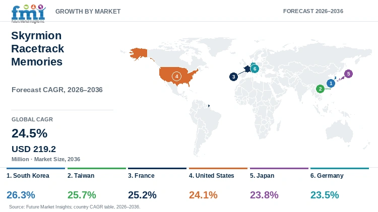
South Korean foundry pilot lines are projected to lead the six major skyrmion racetrack memories countries with a 26.3% annual growth pace through 2036, followed closely by Taiwanese wafer fabs (25.7%) and French defense spintronics hubs (25.2%) before the United States (24.1%) and both Japan (23.8%) and Germany (23.5%). National CHIPS subsidies alongside 300-millimeter multi-cathode sputtering capacity and defense satellite procurement budgets govern these country growth differentials.
Table 7: Country CAGR and Primary Growth Levers for the Skyrmion Racetrack Memories Market (CAGR percentage and operational drivers), 2026 to 2036
| Country | CAGR (2026 to 2036) | Primary Growth Lever |
|---|---|---|
| South Korea | 26.3% | K-Chips Act foundry BEOL spintronic pilot lines and AI memory-semantic cache integration |
| Taiwan | 25.7% | 3nm/4nm FinFET wafer shuttle ecosystems and CoWoS/FCBGA high-pin-count packaging dominance |
| France | 25.2% | France 2030 PEPR Spin national program and CEA/Thales defense lab-to-fab commercialization |
| United States | 24.1% | CHIPS Act microelectronics commons and DoD radiation-hardened satellite cache procurement |
| Japan | 23.8% | METI/NEDO spintronic wafer tooling grants and ultra-clean magnetic sputtering target supply |
| Germany | 23.5% | Multi-cathode TIMARIS PVD cluster manufacturing and Fraunhofer spintronic wafer services |
Source: Future Market Insights analysis
South Korea Skyrmion Racetrack Memories Market Outlook (2026 to 2036)
Aggressive capital deployment by domestic memory conglomerates into post-DRAM spintronic architectures positions South Korea at the forefront of commercial skyrmion racetrack adoption. In January 2025, the South Korean Ministry of Science and ICT announced a record KRW 24.8 trillion national research and development budget prioritizing next-generation semiconductor memory and quantum-spintronic hardware [12]. Backed by these sovereign foundry incentives, South Korean skyrmion racetrack memory sales are projected to climb 26.3% annually from 2026 through 2036. However, commercial engineering teams confront severe thermal budget incompatibilities between high-temperature CMOS interconnect anneals and ultrathin cobalt-iron-boron chiral superlattices. Domestic fabs are overcoming this barrier by installing dedicated low-temperature krypton physical vapor deposition modules inside Hwaseong and Pyeongtaek pilot lines.
Key takeaway: In South Korea, sovereign semiconductor R&D budgets and 300-millimeter memory foundry pilot lines sustain a projected 26.3% annual growth trajectory through 2036.
Taiwan Skyrmion Racetrack Memories Market Outlook (2026 to 2036)
Unmatched contract foundry density in Hsinchu and Tainan makes Taiwan the primary fabrication hub for 4nm and 5nm FinFET back-end-of-line spintronic memory shuttles. In September 2025, the Ministry of Economic Affairs presented 3D chip modules and heterogeneous integration technologies at SEMICON Taiwan to strengthen Taiwan's advanced semiconductor innovation chain [13]. Supported by world-leading flip-chip ball grid array assembly houses, Taiwanese skyrmion racetrack turnover is forecast to advance at a 25.7% yearly clip until 2036. Even so, fabless memory developers face multi-month multi-project wafer queue times and steep mask charges on sub-5-nanometer nodes. Taiwanese foundries are addressing access bottlenecks by offering standardized spintronic back-end interposer shuttles for AI accelerator vendors.
Key takeaway: In Taiwan, contract FinFET foundry ecosystems and high-pin-count FCBGA packaging infrastructure drive an estimated 25.7% compound annual expansion through 2036.
France Skyrmion Racetrack Memories Market Outlook (2026 to 2036)
Deep public-private collaboration between national condensed-matter laboratories and defense aerospace primes gives France Europe's strongest skyrmion device commercialization pipeline. In May 2026, the French Alternative Energies and Atomic Energy Commission (CEA) joined the European Chips Joint Undertaking pilot line consortium alongside France 2030 spintronics laboratories in Grenoble and Saclay [14]. This lab-to-fab pipeline is anticipated to lift French skyrmion racetrack memory expenditure by 25.2% per year between 2026 and 2036. Nevertheless, transitioning chiral magnetic nanowires from 200-millimeter research wafers onto high-volume 300-millimeter commercial CMOS lines remains constrained by limited domestic FinFET foundry capacity. French defense electronics suppliers mitigate this constraint by licensing radiation-hardened skyrmion cache macros for sovereign satellite processors.
Key takeaway: In France, European Chips pilot-line participation and defense avionics qualification programs foster a predicted 25.2% annual growth rate through 2036.
United States Skyrmion Racetrack Memories Market Outlook (2026 to 2036)
Defense satellite modernization and federal microelectronics common-foundry grants anchor commercial skyrmion racetrack memory procurement across the United States. During October 2026, federal Commerce Department and NIST officials finalized an amended CHIPS agreement with GlobalFoundries to expand domestic semiconductor fabrication in New York and Vermont for aerospace and defense systems [15]. Fueled by radiation-hardened space cache upgrades, United States skyrmion racetrack revenues are expected to progress at a 24.1% annual pace through 2036. Still, strict International Traffic in Arms Regulations export controls and protracted MIL-PRF-38535 space qualification cycles lengthen commercial sales lead times for startup memory houses. Domestic spintronic foundries offset long defense qualification cycles by supplying commercial Compute Express Link persistent memory evaluation boards.
Key takeaway: In the United States, federal CHIPS foundry investments and radiation-hardened defense satellite procurement underpin an estimated 24.1% compound annual growth rate through 2036.
Japan Skyrmion Racetrack Memories Market Outlook (2026 to 2036)
Precision magnetic read-head engineering and ultra-pure sputtering target metallurgy give Japan a structural advantage in chiral multilayer stack fabrication. In October 2026, Japan's Ministry of Economy, Trade and Industry approved new capital grants under its Strategic Investment Initiative to scale domestic advanced semiconductor and non-volatile memory manufacturing [16]. Reinforced by close partnerships between storage device makers and national spintronics institutes, Japanese skyrmion racetrack revenue is projected to rise 23.8% each year through 2036. However, a shortage of domestic sub-5-nanometer logic foundries forces Japanese spintronic device teams to validate high-speed SerDes interfaces through overseas wafer shuttles. Domestic manufacturers are narrowing this gap by integrating skyrmion shift registers with cryogenic optical interconnects and automotive radar microcontrollers.
Key takeaway: In Japan, METI semiconductor capital subsidies and magnetic thin-film tooling leadership sustain a forecast 23.8% yearly expansion pace until 2036.
Germany Skyrmion Racetrack Memories Market Outlook (2026 to 2036)
World-leading vacuum physical vapor deposition equipment manufacturing and applied microelectronics research institutes anchor Germany's position in the global skyrmion supply chain. In September 2026, Fraunhofer IPMS convened its Fast Innovation through Research in Semiconductor Technologies symposium in Dresden to advance 300-millimeter back-end-of-line magnetic and ferroelectric memory wafer services [17]. Backed by industrial automation and automotive edge-AI demand, German skyrmion racetrack memory billings are predicted to climb 23.5% annually through 2036. Even so, high industrial electricity tariffs and stringent European cleanroom chemical regulations elevate wafer processing overhead for mid-sized specialty fabs. German equipment and foundry providers counter rising utility costs by exporting multi-cathode TIMARIS sputtering systems and pre-validated SAF CoFeB/Pt/Ir wafer templates.
Key takeaway: In Germany, 300-millimeter Fraunhofer wafer services and modular PVD sputtering equipment exports drive a projected 23.5% annual growth rate through 2036.
Full report country CAGRs cover: North America; Latin America; Western Europe; Eastern Europe; East Asia; South Asia and Pacific; Middle East and Africa.
Who are the notable companies in the skyrmion racetrack memories market?
Everspin Technologies, Inc., TDK Corporation (Headway Technologies), Western Digital Corporation / Kioxia, IBM Research / Samsung Spintronics Alliance, Singulus Technologies AG, Thales Group, Applied Materials, Inc., and NVE Corporation are the notable companies in the skyrmion racetrack memories market.
Supplier participation across the skyrmion racetrack memories ecosystem spans direct chiral nanowire R&D pioneers, adjacent magnetoresistive foundry and spintronic sensor manufacturers, and multi-cathode physical vapor deposition equipment builders. Direct skyrmion and racetrack shift-register pioneers including the IBM Research / Samsung Spintronics Alliance and Thales Group alongside TDK Corporation (Headway Technologies) engineer synthetic antiferromagnetic nanowire shift registers and chiral skyrmion neuromorphic reservoirs. Adjacent commercial spintronic memory and sensor producers such as Everspin Technologies, Inc. and Western Digital Corporation / Kioxia together with NVE Corporation manufacture conventional toggle or spin-transfer-torque MRAM and TMR sensors that provide foundational magnetic tunnel junction readout and radiation-hardened back-end infrastructure without yet marketing standalone skyrmion racetrack chips. Meanwhile, Singulus Technologies AG and Applied Materials, Inc. supply the ultra-high-vacuum multi-cathode sputtering clusters required to deposit sub-nanometer platinum and iridium interfaces.
- Direct Skyrmion Racetrack & Chiral Spintronics R&D Leaders: The IBM Research / Samsung Spintronics Alliance and Thales Group alongside TDK Corporation (Headway Technologies) develop synthetic antiferromagnetic domain-wall shift registers and room-temperature skyrmion neuromorphic prototype arrays.
- Adjacent Spintronic Foundry & MTJ Readout Infrastructure Providers: Everspin Technologies, Inc. and Western Digital Corporation / Kioxia together with NVE Corporation supply adjacent commercial toggle/STT-MRAM foundry processes and high-reliability TMR readout sensors adaptable to nanowire shift registers.
- Multi-Cathode PVD & Spintronic Stack Tooling Suppliers: Singulus Technologies AG and Applied Materials, Inc. manufacture automated physical vapor deposition and atomic-layer etching systems for synthetic antiferromagnetic CoFeB/Pt/Ir superlattices.
Competitive Benchmarking: Skyrmion Racetrack Memories Market
Table 8: Competitive Benchmarking for the Skyrmion Racetrack Memories Market (qualitative capability ratings), 2026
| Company | Chiral Racetrack R&D | CMOS / MTJ Integration | Rad-Hard / AI Readiness | Global Fab Reach |
|---|---|---|---|---|
| IBM Research / Samsung Spintronics Alliance | High | High | High | High |
| Thales Group | High | Medium | High | Medium |
| TDK Corporation (Headway Technologies) | High | High | Medium | High |
| Singulus Technologies AG | High | Medium | Medium | High |
| Applied Materials, Inc. | Medium | High | Medium | High |
| Western Digital Corporation / Kioxia | Medium | High | Medium | High |
| Everspin Technologies, Inc. | Medium | High | High | Medium |
| NVE Corporation | Medium | Medium | High | Medium |
Scoring basis: Chiral Racetrack R&D earns a High rating only where an organization demonstrates direct synthetic antiferromagnetic domain-wall or chiral skyrmion shift-register prototypes and PVD multilayer stacks, whereas Medium denotes adjacent STT/toggle-MRAM foundry or spintronic sensor providers that do not yet market standalone skyrmion hardware. CMOS / MTJ Integration evaluates documented 200-millimeter or 300-millimeter back-end-of-line magnetic tunnel junction readout and FinFET peripheral integration. Rad-Hard / AI Readiness reflects active aerospace radiation qualification or neuromorphic edge computing development programs.
Key Developments in the Skyrmion Racetrack Memories Market
- In June 2026, TDK Corporation announced the construction of a new advanced magnetic and spintronic sensor manufacturing facility in Japan to expand production capacity for AI and industrial edge hardware [18].
- In March 2026, IBM Corporation released a new blueprint for quantum-centric supercomputing and low-power memory interconnect architectures to unify cryogenic and spintronic memory tiers [19].
- In January 2026, Thales Group deployed its secure post-quantum operating system and hardware protection architecture inside Samsung Electronics' CES-winning security chip for defense and enterprise edge platforms [20].
Key Players in the Skyrmion Racetrack Memories Market
Spintronic Foundry & Non-Volatile Memory Platforms
- Everspin Technologies, Inc.
- IBM Research / Samsung Spintronics Alliance
- Western Digital Corporation / Kioxia
Chiral Magnetic Multilayer & Defense Device Specialists
- TDK Corporation (Headway Technologies)
- Thales Group
- NVE Corporation
Multi-Cathode PVD & Spintronic Stack Tooling Suppliers
- Singulus Technologies AG
- Applied Materials, Inc.
Skyrmion Racetrack Memories Market - Report Scope
Table 9: Report Scope for the Skyrmion Racetrack Memories Market (coverage fields and definitions), 2026 to 2036
| Coverage field | Report scope |
|---|---|
| Market breakdown | Chiral Magnetic Multilayer Stack; Nucleation & Readout Mechanism; Target Computing Application; Package Substrate Size; Process Node; Region |
| Quantitative Units | USD Million |
| Market Definition | Includes foundry, device manufacturer, and specialty tooling revenue directly attributable to skyrmion racetrack memory dies, multi-project wafer (MPW) spintronic shuttles, radiation-hardened chiral nanowire cache modules, and stochastic skyrmion neuromorphic co-processors sold within the listed segmentation. Category Scope Note: The valuation strictly captures chiral magnetic domain-wall and skyrmion shift-register memory hardware and dedicated spintronic stack engineering services, excluding commodity planar toggle MRAM, standalone STT-MRAM chips lacking racetrack shift registers, and mechanical hard-disk drives. |
| Regions Covered | North America; Latin America; Western Europe; Eastern Europe; East Asia; South Asia and Pacific; Middle East and Africa |
| Countries Covered | South Korea, Taiwan, France, United States, Japan, Germany, and additional countries in the full report |
| Key Companies Covered | Everspin Technologies, Inc., TDK Corporation (Headway Technologies), Western Digital Corporation / Kioxia, IBM Research / Samsung Spintronics Alliance, Singulus Technologies AG, Thales Group, Applied Materials, Inc., NVE Corporation |
| Forecast Period | 2026 to 2036 |
| Approach | Primary and secondary research with rigorous market triangulation. |
Skyrmion Racetrack Memories Market - Research Methodology
Table 10: Research Methodology for the Skyrmion Racetrack Memories Market (research methods and approach), 2026 edition
| Method | Approach |
|---|---|
| Primary Research | Primary interviews were conducted with spintronic foundry process architects, PVD sputtering equipment engineers, radiation-hardened satellite avionics directors, neuromorphic chip designers, and defense microelectronics buyers to validate chiral stack yields, SOT current thresholds, and wafer shuttle pricing. |
| Secondary Research | Secondary research included company annual reports, investor presentations, NIST and CHIPS for America program disclosures, CEA/CNRS European Chips publications, METI and MSIT semiconductor budget registries, Physical Review B and Reviews of Modern Physics papers, and verified corporate press releases. |
| Market Sizing and Forecasting | Market sizing and forecasting for the 2026 to 2036 period were developed using top-down and bottom-up models reconciling 200mm/300mm spintronic wafer shuttle allocations, defense radiation-hardened cache contracts, and neuromorphic accelerator tape-outs. |
| Data Triangulation and Validation | Estimates are triangulated against multi-cathode PVD tool installations, sovereign microelectronics grant disbursements, and foundry BEOL shuttle schedules to ensure high accuracy without double counting standard STT-MRAM categories. |
| Country Forecasting Model | Country-level CAGRs are projected via FMI's semiconductor spintronics econometric model, calibrating national growth rates against the 24.5% global baseline using sovereign CHIPS funding disbursements, 300mm FinFET foundry capacity, and defense space electronics budgets. |
| Operational Benchmark Traceability | Operational benchmarks (300mm-equivalent wafer shuttles, effective skyrmion bit pitch, and SOT current density) represent modeled scenario ranges synthesized from NIST spintronic metrology data, Fraunhofer IPMS wafer specifications, and foundry shuttle disclosures. |
Skyrmion Racetrack Memories Market by Segments
Skyrmion Racetrack Memories Market segmented by Chiral Magnetic Multilayer Stack:
- Synthetic Antiferromagnetic (SAF) CoFeB/Pt/Ir Heavy-Metal Tracks
- Ferrimagnetic GdFeCo Zero-Skyrmion-Hall-Angle Nanowires
- 2D Van der Waals Ferromagnet (Fe3GeTe2) Heterostructures
Skyrmion Racetrack Memories Market segmented by Nucleation & Readout Mechanism:
- Spin-Orbit Torque (SOT) Current-Driven + MTJ Tunnel Readout
- Voltage-Controlled Magnetic Anisotropy (VCMA) Gated Tracks
- Topological Hall-Effect & Optical Kerr Readout Arrays
Skyrmion Racetrack Memories Market segmented by Target Computing Application:
- Radiation-Hardened Space & Defense Non-Volatile Cache
- Stochastic & Brownian Reservoir Neuromorphic Accelerators
- Ultra-Dense Last-Level CPU/GPU Working Memory Replacement
Skyrmion Racetrack Memories Market segmented by Package Substrate Size:
- 55x55 mm to 75x75 mm FCBGA High-Pin-Count
- <55x55 mm Compact Edge Switch Package
- Wafer-Level Known-Good-Die (KGD) Cryogenic & 2.5D Interposers
Skyrmion Racetrack Memories Market segmented by Process Node:
- 4nm / 5nm FinFET Low-Power SerDes Node
- 3nm Advanced SerDes Node
- 14nm to 28nm Rad-Hard CMOS Back-End-of-Line (BEOL) Node
Skyrmion Racetrack Memories Market by Region
- North America
- United States
- Canada
- Latin America
- Brazil
- Mexico
- Argentina
- Chile
- Western Europe
- Germany
- France
- United Kingdom
- Italy
- Spain
- Benelux
- Nordics
- Eastern Europe
- Poland
- Czech Republic
- Romania
- Hungary
- East Asia
- China
- Japan
- South Korea
- South Asia and Pacific
- India
- ASEAN
- Australia and New Zealand
- Middle East and Africa
- GCC Countries
- South Africa
- Türkiye
- Israel
Research Sources and Bibliography
- [1] National Institute of Standards and Technology (NIST). (2025, August 18). NIST Researchers Demonstrate that Superconducting Neural Networks Can Learn on Their Own. U.S. Department of Commerce.
- [2] National Institute of Standards and Technology (NIST). (2026, May 21). Department of Commerce Announces Letters of Intent With 9 Companies for $2 Billion to Accelerate U.S. Leadership in Quantum Computing. U.S. Department of Commerce.
- [3] Kharlan, J., Zelent, M., Guslienko, K., Golub, V. O., & Kłos, J. W. (2025, December 10). Stabilization of the skyrmion in a hybrid magnetic-superconducting nanostucture. Physical Review B, 112(22), 224418 (American Physical Society).
- [4] Silicon Semiconductor & Singulus Technologies AG. (2026, January 05). SINGULUS TECHNOLOGIES receives further order for modular vacuum coating system. Silicon Semiconductor News.
- [5] Hlushchenko, A. V., Bratchenko, M. I., & Chechkin, A. V. (2026, May 18). Stochastic dynamics of skyrmions on a racetrack: Impact of equilibrium and nonequilibrium noise. Physical Review B, 113(18), L180407 (American Physical Society).
- [6] Banik, S., & Nandy, A. K. (2025, October 21). Skyrmion-antiskyrmion lattice: A net-zero topological phase in low-symmetry frustrated chiral magnets. Physical Review B, 112(14), L140404 (American Physical Society).
- [7] Samsung Electronics Co., Ltd. (2026, August 05). Samsung Unveils Next-Gen 3D-Memory Vision at FMS 2026, Charting the Future of AI Infrastructure. Samsung Global Newsroom.
- [8] Applied Materials, Inc. (2026, October 12). Applied Materials Unveils $5 Billion EPIC Center in Silicon Valley to Accelerate Semiconductor Innovation for the AI Era. Applied Materials Newsroom.
- [9] Petrović, A. P., Psaroudaki, C., Fischer, P., Garst, M., & Panagopoulos, C. (2025, July 08). Colloquium: Quantum properties and functionalities of magnetic skyrmions. Reviews of Modern Physics, 97(3), 031001 (American Physical Society).
- [10] Vizarim, N. P., Bellizotti Souza, J. C., Reichhardt, C. J. O., Reichhardt, C., Venegas, P. A., & Béron, F. (2025, June 26). Skyrmion-skyrmionium phase separation and laning transitions via spin-orbit torque currents. Physical Review B, 111(21), 214438 (American Physical Society).
- [11] Go, G., & Kim, S. K. (2026, February 11). Magnetoelastic Coupling-Driven Chiral Spin Textures: A Skyrmion-Antiskyrmion-like Array. Physical Review Letters, 136(6), 066702 (American Physical Society).
- [12] Ministry of Science and ICT (MSIT). (2025, January 14). Major R&D Budget for 2025 Set to Be KRW 24.8 Trillion, the Largest in History. Ministry of Science and ICT Republic of Korea.
- [13] Ministry of Economic Affairs (MOEA). (2025, September 12). MOEA Showcases Silicon Photonics and 3D Chip Modules to Strengthen Taiwan's Semiconductor Innovation Chain. Ministry of Economic Affairs, R.O.C.
- [14] VTT Technical Research Centre of Finland Ltd. & CEA France. (2026, May 11). The SUPREME quantum project enforces Finland's leading role in European quantum research. VTT News and Ideas (European Chips JU Consortium with CEA France).
- [15] National Institute of Standards and Technology (NIST). (2026, October 14). Department of Commerce Announces Agreement with GlobalFoundries to Amend Its Existing CHIPS Program Award and Reallocate $955 Million to Accelerate Investments in Silicon Photonics, Silicon-Germanium, and Advanced Packaging. U.S. Department of Commerce.
- [16] Ministry of Economy, Trade and Industry (METI). (2026, October 15). Semiconductor Manufacturing Project to be Implemented under the Japan-U.S. Strategic Investment Initiative. Ministry of Economy, Trade and Industry Japan.
- [17] Fraunhofer Institute for Photonic Microsystems (IPMS). (2026, September 30). FIRST – Fast Innovation through Research in Semiconductor Technologies. Fraunhofer-Gesellschaft.
- [18] TDK Corporation. (2026, June 01). TDK drives the growth of sensor business with new factory in Japan. TDK Corporation News Center.
- [19] IBM Corporation. (2026, March 12). IBM Releases a New Blueprint for Quantum-Centric Supercomputing. IBM Newsroom.
- [20] Thales Group. (2026, January 06). Thales powers CES-winning post-quantum chip from Samsung Electronics. Thales Group Press Releases.
- [21] TDK Corporation. (2025, December 09). TDK unveils physical AI technologies that enhance devices and experiences — “In Everything, Better” at CES 2026. TDK Corporation News Center.
This bibliography is provided for reader reference and is not exhaustive. The full report contains the complete reference list and detailed citations.
This Report Answers
- How large is the skyrmion racetrack memories market in 2026 and what is forecast for 2036?
- Which radiation-hardening and AI memory-wall pressures support skyrmion racetrack adoption?
- Why do Synthetic Antiferromagnetic (SAF) CoFeB/Pt/Ir Heavy-Metal Tracks lead stack selection?
- Why does Spin-Orbit Torque (SOT) Current-Driven + MTJ Tunnel Readout lead readout mechanisms?
- How do national growth rates differ across South Korea, Taiwan, France, the United States, Japan, and Germany?
- Which foundries, spintronic chipmakers, and PVD equipment suppliers lead the ecosystem today?
- What technical barriers restrict nanowire bit-position accuracy and SOT current reduction?
- What should satellite avionics and AI hardware buyers evaluate before qualifying skyrmion memory?
Frequently Asked Questions
How big is the skyrmion racetrack memories market in 2026, and what is forecast for 2036?
Global skyrmion racetrack memories turnover is estimated at USD 24.5 million in 2026 (rising from USD 19.8 million in 2025) and is projected to reach USD 219.2 million by 2036 as aerospace and AI hardware architects adopt topologically protected nanowire shift registers.
What is the CAGR for the skyrmion racetrack memories market from 2026 to 2036?
As per FMI, worldwide skyrmion racetrack memory expenditure is forecast to expand at a 24.5% annual rate between 2026 and 2036, generating USD 194.7 million in incremental foundry shuttle and radiation-hardened cache sales.
Which chiral magnetic multilayer stack segment leads the skyrmion racetrack memories market?
Synthetic Antiferromagnetic (SAF) CoFeB/Pt/Ir Heavy-Metal Tracks are projected to capture 58.6% of 2026 multilayer stack demand because antiparallel exchange coupling cancels lateral skyrmion Hall deflection at high domain speeds.
Which nucleation and readout mechanism leads the skyrmion racetrack memories market?
Spin-Orbit Torque (SOT) Current-Driven + MTJ Tunnel Readout is estimated to command 66.4% of 2026 readout share owing to sub-nanosecond current-driven domain shifting paired with high-contrast magnetic tunnel junction sensing.
Which country exhibits the fastest expansion in the skyrmion racetrack memories market?
FMI analysis indicates that South Korea is projected to lead the six major semiconductor nations at 26.3% annually from 2026 to 2036, backed by sovereign semiconductor R&D budgets and 300-millimeter memory foundry pilot lines.
Who are the key players in the skyrmion racetrack memories market?
Leading participants include Everspin Technologies, Inc., TDK Corporation (Headway Technologies), Western Digital Corporation / Kioxia, IBM Research / Samsung Spintronics Alliance, Singulus Technologies AG, Thales Group, Applied Materials, Inc., and NVE Corporation.
Preview the report firsthand - request a free sample
Get SampleGet the brochure for pricing and purchase details.
Get PDFTable of Content
- Key Takeaways
- Market Size and CAGR
- Top Growth Driver
- Fastest Growing Segment
- Leading Region
- Key Companies
- Emerging Opportunities
- Executive Summary
- Global Market Outlook
- Demand-side Trends
- Supply-side Trends
- Technology Roadmap Analysis
- Analysis and Recommendations
- Analyst Perspective (What is happening? Why now? What should investors know?)
- Key Questions Answered
- How large is the market?
- What is the CAGR?
- What are key trends?
- Which region dominates?
- Who are the leaders?
- Market Overview
- Market Coverage / Taxonomy
- Market Definition / Scope / Limitations
- Research Methodology
- Chapter Orientation
- Analytical Lens and Working Hypotheses
- Market Structure, Signals, and Trend Drivers
- Benchmarking and Cross-market Comparability
- Market Sizing, Forecasting, and Opportunity Mapping
- Research Design and Evidence Framework
- Desk Research Programme (Secondary Evidence)
- Expert Input and Fieldwork (Primary Evidence)
- Tooling, Models, and Reference Databases
- Data Engineering and Model Build
- Quality Assurance and Audit Trail
- Market Background
- Market Dynamics (Drivers, Restraints, Opportunity, Trends)
- Scenario Forecast (Optimistic, Likely, Conservative)
- Impact Analysis
- AI Impact
- Sustainability Impact
- Regulatory Impact
- Technology Impact
- Consumer / Buyer Analysis
- Purchase Drivers
- Adoption Barriers
- Buyer Journey
- Opportunity Map Analysis
- Product Life Cycle Analysis
- Supply Chain Analysis
- Investment Feasibility Matrix
- Value Chain Analysis
- PESTLE and Porter's Analysis
- Regulatory Landscape
- Regional Parent Market Outlook
- Production and Consumption Statistics
- Import and Export Statistics
- Global Market Analysis and Forecast, 2021 to 2036
- Historical Market Size Value (USD Million) Analysis, 2021 to 2025
- Current and Future Market Size Value (USD Million) Projections, 2026 to 2036
- Y-o-Y Growth Trend Analysis
- Absolute $ Opportunity Analysis
- Global Market Pricing Analysis, 2021 to 2036
- Global Market Analysis and Forecast, By Chiral Magnetic Multilayer Stack, 2021 to 2036
- Introduction / Key Findings
- Historical Market Size Value (USD Million) Analysis By Chiral Magnetic Multilayer Stack, 2021 to 2025
- Current and Future Market Size Value (USD Million) Analysis and Forecast By Chiral Magnetic Multilayer Stack, 2026 to 2036
- Synthetic Antiferromagnetic (SAF) CoFeB/Pt/Ir Heavy-Metal Tracks
- Ferrimagnetic GdFeCo Zero-Skyrmion-Hall-Angle Nanowires
- 2D Van der Waals Ferromagnet (Fe3GeTe2) Heterostructures
- Y-o-Y Growth Trend Analysis By Chiral Magnetic Multilayer Stack, 2021 to 2025
- Absolute $ Opportunity Analysis By Chiral Magnetic Multilayer Stack, 2026 to 2036
- Global Market Analysis and Forecast, By Nucleation & Readout Mechanism, 2021 to 2036
- Introduction / Key Findings
- Historical Market Size Value (USD Million) Analysis By Nucleation & Readout Mechanism, 2021 to 2025
- Current and Future Market Size Value (USD Million) Analysis and Forecast By Nucleation & Readout Mechanism, 2026 to 2036
- Spin-Orbit Torque (SOT) Current-Driven + MTJ Tunnel Readout
- Voltage-Controlled Magnetic Anisotropy (VCMA) Gated Tracks
- Topological Hall-Effect & Optical Kerr Readout Arrays
- Y-o-Y Growth Trend Analysis By Nucleation & Readout Mechanism, 2021 to 2025
- Absolute $ Opportunity Analysis By Nucleation & Readout Mechanism, 2026 to 2036
- Global Market Analysis and Forecast, By Target Computing Application, 2021 to 2036
- Introduction / Key Findings
- Historical Market Size Value (USD Million) Analysis By Target Computing Application, 2021 to 2025
- Current and Future Market Size Value (USD Million) Analysis and Forecast By Target Computing Application, 2026 to 2036
- Radiation-Hardened Space & Defense Non-Volatile Cache
- Stochastic & Brownian Reservoir Neuromorphic Accelerators
- Ultra-Dense Last-Level CPU/GPU Working Memory Replacement
- Y-o-Y Growth Trend Analysis By Target Computing Application, 2021 to 2025
- Absolute $ Opportunity Analysis By Target Computing Application, 2026 to 2036
- Global Market Analysis and Forecast, By Package Substrate Size, 2021 to 2036
- Introduction / Key Findings
- Historical Market Size Value (USD Million) Analysis By Package Substrate Size, 2021 to 2025
- Current and Future Market Size Value (USD Million) Analysis and Forecast By Package Substrate Size, 2026 to 2036
- 55x55 mm to 75x75 mm FCBGA High-Pin-Count
- <55x55 mm Compact Edge Switch Package
- Wafer-Level Known-Good-Die (KGD) Cryogenic & 2.5D Interposers
- Y-o-Y Growth Trend Analysis By Package Substrate Size, 2021 to 2025
- Absolute $ Opportunity Analysis By Package Substrate Size, 2026 to 2036
- Global Market Analysis and Forecast, By Process Node, 2021 to 2036
- Introduction / Key Findings
- Historical Market Size Value (USD Million) Analysis By Process Node, 2021 to 2025
- Current and Future Market Size Value (USD Million) Analysis and Forecast By Process Node, 2026 to 2036
- 4nm / 5nm FinFET Low-Power SerDes Node
- 3nm Advanced SerDes Node
- 14nm to 28nm Rad-Hard CMOS Back-End-of-Line (BEOL) Node
- Y-o-Y Growth Trend Analysis By Process Node, 2021 to 2025
- Absolute $ Opportunity Analysis By Process Node, 2026 to 2036
- Global Market Analysis and Forecast, By Region, 2021 to 2036
- Introduction
- Historical Market Size Value (USD Million) Analysis By Region, 2021 to 2025
- Current Market Size Value (USD Million) Analysis and Forecast By Region, 2026 to 2036
- North America
- Latin America
- Western Europe
- Eastern Europe
- East Asia
- South Asia and Pacific
- Middle East and Africa
- Market Attractiveness Analysis By Region
- North America Market Analysis and Forecast, By Country, 2021 to 2036
- Historical Market Size Value (USD Million) Trend Analysis By Market Taxonomy, 2021 to 2025
- Market Size Value (USD Million) Forecast By Market Taxonomy, 2026 to 2036
- By Country
- United States
- Canada
- By Chiral Magnetic Multilayer Stack
- By Nucleation & Readout Mechanism
- By Target Computing Application
- By Package Substrate Size
- By Process Node
- By Country
- Market Attractiveness Analysis
- By Country
- By Chiral Magnetic Multilayer Stack
- By Nucleation & Readout Mechanism
- By Target Computing Application
- By Package Substrate Size
- By Process Node
- Key Takeaways
- Latin America Market Analysis and Forecast, By Country
- Historical Market Size Value (USD Million) Trend Analysis By Market Taxonomy, 2021 to 2025
- Market Size Value (USD Million) Forecast By Market Taxonomy, 2026 to 2036
- By Country
- Brazil
- Mexico
- Argentina
- Chile
- By Chiral Magnetic Multilayer Stack
- By Nucleation & Readout Mechanism
- By Target Computing Application
- By Package Substrate Size
- By Process Node
- By Country
- Market Attractiveness Analysis
- By Country
- By Chiral Magnetic Multilayer Stack
- By Nucleation & Readout Mechanism
- By Target Computing Application
- By Package Substrate Size
- By Process Node
- Key Takeaways
- Western Europe Market Analysis and Forecast, By Country
- Historical Market Size Value (USD Million) Trend Analysis By Market Taxonomy, 2021 to 2025
- Market Size Value (USD Million) Forecast By Market Taxonomy, 2026 to 2036
- By Country
- Germany
- France
- United Kingdom
- Italy
- Spain
- Benelux
- Nordics
- By Chiral Magnetic Multilayer Stack
- By Nucleation & Readout Mechanism
- By Target Computing Application
- By Package Substrate Size
- By Process Node
- By Country
- Market Attractiveness Analysis
- By Country
- By Chiral Magnetic Multilayer Stack
- By Nucleation & Readout Mechanism
- By Target Computing Application
- By Package Substrate Size
- By Process Node
- Key Takeaways
- Eastern Europe Market Analysis and Forecast, By Country
- Historical Market Size Value (USD Million) Trend Analysis By Market Taxonomy, 2021 to 2025
- Market Size Value (USD Million) Forecast By Market Taxonomy, 2026 to 2036
- By Country
- Poland
- Czech Republic
- Romania
- Hungary
- By Chiral Magnetic Multilayer Stack
- By Nucleation & Readout Mechanism
- By Target Computing Application
- By Package Substrate Size
- By Process Node
- By Country
- Market Attractiveness Analysis
- By Country
- By Chiral Magnetic Multilayer Stack
- By Nucleation & Readout Mechanism
- By Target Computing Application
- By Package Substrate Size
- By Process Node
- Key Takeaways
- East Asia Market Analysis and Forecast, By Country
- Historical Market Size Value (USD Million) Trend Analysis By Market Taxonomy, 2021 to 2025
- Market Size Value (USD Million) Forecast By Market Taxonomy, 2026 to 2036
- By Country
- China
- Japan
- South Korea
- By Chiral Magnetic Multilayer Stack
- By Nucleation & Readout Mechanism
- By Target Computing Application
- By Package Substrate Size
- By Process Node
- By Country
- Market Attractiveness Analysis
- By Country
- By Chiral Magnetic Multilayer Stack
- By Nucleation & Readout Mechanism
- By Target Computing Application
- By Package Substrate Size
- By Process Node
- Key Takeaways
- South Asia and Pacific Market Analysis and Forecast, By Country
- Historical Market Size Value (USD Million) Trend Analysis By Market Taxonomy, 2021 to 2025
- Market Size Value (USD Million) Forecast By Market Taxonomy, 2026 to 2036
- By Country
- India
- ASEAN
- Australia and New Zealand
- By Chiral Magnetic Multilayer Stack
- By Nucleation & Readout Mechanism
- By Target Computing Application
- By Package Substrate Size
- By Process Node
- By Country
- Market Attractiveness Analysis
- By Country
- By Chiral Magnetic Multilayer Stack
- By Nucleation & Readout Mechanism
- By Target Computing Application
- By Package Substrate Size
- By Process Node
- Key Takeaways
- Middle East and Africa Market Analysis and Forecast, By Country
- Historical Market Size Value (USD Million) Trend Analysis By Market Taxonomy, 2021 to 2025
- Market Size Value (USD Million) Forecast By Market Taxonomy, 2026 to 2036
- By Country
- GCC Countries
- South Africa
- Türkiye
- Israel
- By Chiral Magnetic Multilayer Stack
- By Nucleation & Readout Mechanism
- By Target Computing Application
- By Package Substrate Size
- By Process Node
- By Country
- Market Attractiveness Analysis
- By Country
- By Chiral Magnetic Multilayer Stack
- By Nucleation & Readout Mechanism
- By Target Computing Application
- By Package Substrate Size
- By Process Node
- Key Takeaways
- Key Countries Market Analysis
- United States
- Pricing Analysis
- Market Share Analysis, 2025
- By Chiral Magnetic Multilayer Stack
- By Nucleation & Readout Mechanism
- By Target Computing Application
- By Package Substrate Size
- By Process Node
- Canada
- Pricing Analysis
- Market Share Analysis, 2025
- By Chiral Magnetic Multilayer Stack
- By Nucleation & Readout Mechanism
- By Target Computing Application
- By Package Substrate Size
- By Process Node
- Mexico
- Pricing Analysis
- Market Share Analysis, 2025
- By Chiral Magnetic Multilayer Stack
- By Nucleation & Readout Mechanism
- By Target Computing Application
- By Package Substrate Size
- By Process Node
- Brazil
- Pricing Analysis
- Market Share Analysis, 2025
- By Chiral Magnetic Multilayer Stack
- By Nucleation & Readout Mechanism
- By Target Computing Application
- By Package Substrate Size
- By Process Node
- Chile
- Pricing Analysis
- Market Share Analysis, 2025
- By Chiral Magnetic Multilayer Stack
- By Nucleation & Readout Mechanism
- By Target Computing Application
- By Package Substrate Size
- By Process Node
- Germany
- Pricing Analysis
- Market Share Analysis, 2025
- By Chiral Magnetic Multilayer Stack
- By Nucleation & Readout Mechanism
- By Target Computing Application
- By Package Substrate Size
- By Process Node
- United Kingdom
- Pricing Analysis
- Market Share Analysis, 2025
- By Chiral Magnetic Multilayer Stack
- By Nucleation & Readout Mechanism
- By Target Computing Application
- By Package Substrate Size
- By Process Node
- Italy
- Pricing Analysis
- Market Share Analysis, 2025
- By Chiral Magnetic Multilayer Stack
- By Nucleation & Readout Mechanism
- By Target Computing Application
- By Package Substrate Size
- By Process Node
- Spain
- Pricing Analysis
- Market Share Analysis, 2025
- By Chiral Magnetic Multilayer Stack
- By Nucleation & Readout Mechanism
- By Target Computing Application
- By Package Substrate Size
- By Process Node
- France
- Pricing Analysis
- Market Share Analysis, 2025
- By Chiral Magnetic Multilayer Stack
- By Nucleation & Readout Mechanism
- By Target Computing Application
- By Package Substrate Size
- By Process Node
- India
- Pricing Analysis
- Market Share Analysis, 2025
- By Chiral Magnetic Multilayer Stack
- By Nucleation & Readout Mechanism
- By Target Computing Application
- By Package Substrate Size
- By Process Node
- ASEAN
- Pricing Analysis
- Market Share Analysis, 2025
- By Chiral Magnetic Multilayer Stack
- By Nucleation & Readout Mechanism
- By Target Computing Application
- By Package Substrate Size
- By Process Node
- Australia and New Zealand
- Pricing Analysis
- Market Share Analysis, 2025
- By Chiral Magnetic Multilayer Stack
- By Nucleation & Readout Mechanism
- By Target Computing Application
- By Package Substrate Size
- By Process Node
- China
- Pricing Analysis
- Market Share Analysis, 2025
- By Chiral Magnetic Multilayer Stack
- By Nucleation & Readout Mechanism
- By Target Computing Application
- By Package Substrate Size
- By Process Node
- Japan
- Pricing Analysis
- Market Share Analysis, 2025
- By Chiral Magnetic Multilayer Stack
- By Nucleation & Readout Mechanism
- By Target Computing Application
- By Package Substrate Size
- By Process Node
- South Korea
- Pricing Analysis
- Market Share Analysis, 2025
- By Chiral Magnetic Multilayer Stack
- By Nucleation & Readout Mechanism
- By Target Computing Application
- By Package Substrate Size
- By Process Node
- Poland
- Pricing Analysis
- Market Share Analysis, 2025
- By Chiral Magnetic Multilayer Stack
- By Nucleation & Readout Mechanism
- By Target Computing Application
- By Package Substrate Size
- By Process Node
- Hungary
- Pricing Analysis
- Market Share Analysis, 2025
- By Chiral Magnetic Multilayer Stack
- By Nucleation & Readout Mechanism
- By Target Computing Application
- By Package Substrate Size
- By Process Node
- Türkiye
- Pricing Analysis
- Market Share Analysis, 2025
- By Chiral Magnetic Multilayer Stack
- By Nucleation & Readout Mechanism
- By Target Computing Application
- By Package Substrate Size
- By Process Node
- South Africa
- Pricing Analysis
- Market Share Analysis, 2025
- By Chiral Magnetic Multilayer Stack
- By Nucleation & Readout Mechanism
- By Target Computing Application
- By Package Substrate Size
- By Process Node
- Taiwan
- Pricing Analysis
- Market Share Analysis, 2025
- By Chiral Magnetic Multilayer Stack
- By Nucleation & Readout Mechanism
- By Target Computing Application
- By Package Substrate Size
- By Process Node
- United States
- Market Structure Analysis
- Competition Dashboard
- Competition Benchmarking
- Market Share Analysis of Top Players
- By Regional
- By Chiral Magnetic Multilayer Stack
- By Nucleation & Readout Mechanism
- By Target Computing Application
- By Package Substrate Size
- By Process Node
- Emerging Startups
- Innovation Benchmarking
- Competition Analysis
- Competition Deep Dive
- IBM Research / Samsung Spintronics Alliance
- Overview
- Product Portfolio
- Profitability by Market Segments
- Sales Footprint
- Strategy Overview
- Marketing Strategy
- Product Strategy
- Channel Strategy
- Thales Group
- TDK Corporation (Headway Technologies)
- Singulus Technologies AG
- Applied Materials, Inc.
- Western Digital Corporation / Kioxia
- Everspin Technologies, Inc.
- NVE Corporation
- IBM Research / Samsung Spintronics Alliance
- Case Studies
- Success Stories
- Recent Developments
- Competition Deep Dive
- Assumptions & Acronyms Used