About The Report
150mm Probe Station Market Size, Market Forecast and Outlook By FMI
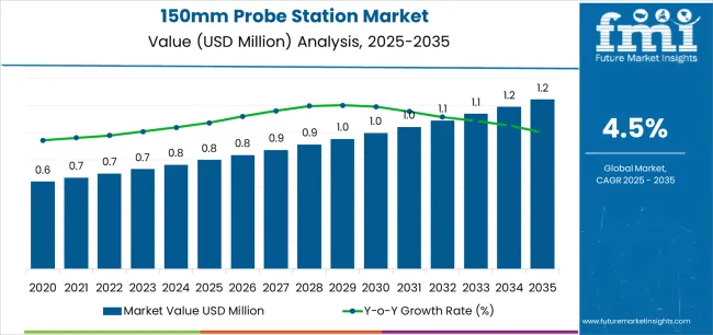
In 2025, the 150mm probe station market was valued at USD 0.80 billion. Based on Future Market Insights' analysis, demand is estimated to grow to USD 0.84 billion in 2026 and USD 1.30 billion by 2036. FMI projects a CAGR of 4.50% during the forecast period.
The market is set to add approximately USD 0.46 billion in absolute terms between 2026 and 2036. 150mm wafer format remains the standard for compound semiconductor (GaN, SiC, GaAs), MEMS, and power device fabrication where 200mm and 300mm transitions have not yet achieved cost-effective yields. University and government research laboratory procurement sustains manual probe station demand, while compound semiconductor production growth in power electronics and RF devices drives semi-automatic configuration adoption.
Summary of 150mm Probe Station Market
- 150mm Probe Station Market Definition
- 150mm probe stations are wafer-level test platforms designed to hold, position, and electrically contact 150mm (6-inch) semiconductor wafers and devices for parametric testing, failure analysis, and device characterization in semiconductor, optoelectronics, and microelectronics research and production environments.
- Demand Drivers in the Market
- Compound semiconductor production on 150mm SiC and GaN wafers for EV power modules and 5G RF amplifiers sustains probe station demand because these materials have not yet migrated to larger wafer formats at production-ready defect densities.
- University and government semiconductor research laboratories procure manual 150mm probe stations as capital equipment for graduate student training, device characterization, and failure analysis workflows where throughput automation is not cost-justified.
- MEMS device fabrication for automotive pressure sensors, accelerometers, and microphones operates predominantly on 150mm wafer lines, with wafer-level parametric testing generating recurring probe station utilization cycles across production shifts.
- Key Segments Analyzed in the FMI Report
- Manual classification: 62.0% share in 2026, reflecting its structural position as the primary category across established procurement channels.
- Semiconductor application: 34.0% share in 2026, reflecting its structural position as the primary category across established procurement channels.
- China: 6.10% compound growth through 2036, indicating concentrated demand acceleration in this geography.
- Analyst Opinion at FMI
- The 150mm probe station market is a capital equipment niche where demand persistence defies the broader semiconductor industry migration toward larger wafer formats. FMI analysts observe that manual classification commands 62.0% share because university research labs and compound semiconductor R&D facilities, which represent the largest customer base for this wafer size, prioritize positioning flexibility and visual access over automated throughput. Semiconductor application at 34.0% share is the lead vertical because compound semiconductor and MEMS device testing generates the highest utilization rate per installed probe station. The 4.5% CAGR reflects the structural reality that 150mm wafer-based production is neither growing rapidly nor declining, as compound semiconductor and MEMS device categories that depend on this format have no near-term economic pathway to larger substrates.
- Strategic Implications / Executive Takeaways
- Probe station manufacturers must develop thermal chuck and cryogenic stage options rated for SiC and GaN device characterization temperatures to capture the compound semiconductor segment requiring high-temperature (up to 300 degrees C) and low-temperature (down to 4K) testing capability.
- University procurement offices should standardize 150mm probe station purchases on modular platforms that accept RF, DC, and optical probe configurations to maximize capital utilization across multi-disciplinary research programs.
- Compound semiconductor fabs scaling 150mm SiC and GaN wafer production should evaluate semi-automatic probe station upgrades to reduce operator-dependent test variability and increase parametric data collection throughput.
150mm Probe Station Market Key Takeaways
| Metric | Details |
|---|---|
| Industry Size (2026) | USD 0.84 Billion |
| Industry Value (2036) | USD 1.30 Billion |
| CAGR (2026 to 2036) | 4.50% |
Source: Future Market Insights, 2026
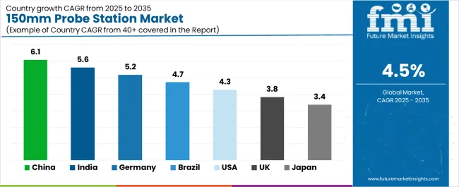
As per FMI, country-level growth rates through 2036 are projected as follows: China at 6.10%, India at 5.60%, Germany at 5.20%, Brazil at 4.70%, USA at 4.30%, UK at 3.80%, Japan at 3.40%. China records the fastest expansion, while mature markets generate steady replacement-cycle demand constrained by saturation in established supply chains.
150mm Probe Station Market Definition
The 150mm probe station market encompasses wafer-level electrical test platforms purpose-built for the 150mm (6-inch) wafer format that remains standard in compound semiconductor, MEMS, and power device fabrication. Equipment configurations span manual probe stations with micropositioner-based needle placement, semi-automatic stations with programmable stage movement, and specialized variants incorporating thermal chucks, RF shielding, and cryogenic cooling. As per FMI, market persistence is structurally linked to the compound semiconductor industry's continued reliance on 150mm substrates, where material defect density and epitaxial growth economics have not yet justified migration to 200mm wafer formats at production scale.
150mm Probe Station Market Inclusions
Market scope covers manual and semi-automatic 150mm probe stations, including thermal chuck variants, RF-capable configurations, and cryogenic probe systems used for wafer-level electrical testing in semiconductor fabs, university research labs, and optoelectronics manufacturing facilities.
150mm Probe Station Market Exclusions
200mm and 300mm probe stations, fully automated production-line wafer probers, standalone probe cards without integrated station platforms, and general-purpose test and measurement instruments not configured for wafer-level probing are excluded.
150mm Probe Station Market Research Methodology
- Primary Research: Analysts conducted structured interviews with procurement managers, product engineers, and distribution channel operators to map purchase decision triggers and specification requirements across key verticals.
- Desk Research: Data collection aggregated regulatory filings, industry standards documentation, patent registries, trade body publications, and company annual reports across all target geographies.
- Market-Sizing and Forecasting: Baseline values derive from a bottom-up aggregation of product shipment volumes and average selling prices, validated against publicly disclosed revenue figures from leading suppliers.
- Data Validation and Update Cycle: Projections are cross-referenced against quarterly earnings data, import-export trade statistics, and industry association production reports to maintain forecast integrity.
Why is the 150 mm Probe Station Market Growing?
The 150 mm probe station market is growing as semiconductor research and legacy wafer-fabrication operations continue to demand accurate on-wafer testing at that wafer size. Probe stations for 150 mm (6 inch) wafers remain relevant in specialised research, older fab lines and niche MEMS or mm-wave device production where migrating entirely to larger wafers is not yet justified. Advanced applications such as THz measurement, mm-wave characterization and compound-semiconductor testing increasingly adopt 150 mm-dedicated probe systems to ensure mechanical stability and high-precision probe placement.
Technological advances in modular probe station design, improved vibration isolation, automated manipulators and integration with advanced instrumentation also support growth of the 150 mm segment. The global resurgence of investment in semiconductor testing, materials research and specialty device production reinforces demand. Constraints include the ongoing industry transition toward larger wafer sizes (200 mm and 300 mm), which reduces the long-term addressable market for 150 mm systems, as well as high capital cost and specialist operator requirements for such equipment.
Which Classification and Application Segments Lead the 150mm Probe Station Market?
The 150mm probe station market is segmented by classification and application. By classification, the market is divided into manual and semi-automatic probe stations. Based on application, the market is categorized into semiconductor, photoelectricity device, micro-electronics, and other precision testing applications. Regionally, the market is divided into Asia Pacific, Europe, North America, and other key regions.
By Classification, the Manual Segment Accounts for the Largest Market Share
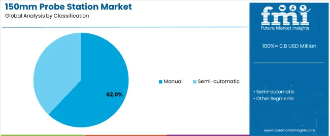
The manual segment holds the leading position in the 150mm probe station market, accounting for approximately 62.0% of the total share in 2025. Manual probe stations remain widely used due to their reliability, cost efficiency, and flexibility in research and development environments where customized probing setups and operator control are essential. These systems allow precise wafer-level electrical measurements while maintaining mechanical simplicity and low maintenance requirements.
The segment’s dominance is supported by extensive adoption in academic laboratories, prototype validation, and low-volume production testing, where automation may not provide proportional cost benefits. Manual stations also offer high adaptability for testing various wafer geometries and materials, particularly in early-stage semiconductor process characterization. Semi-automatic systems, though gaining traction, are typically favored for mid-scale industrial testing requiring enhanced throughput and reduced operator dependency.
Key factors supporting the manual segment include:
- Broad use in research laboratories and low-volume device testing.
- Lower acquisition and maintenance costs compared to automated alternatives.
- High operator control suitable for experimental and prototype validation.
- Ease of integration with a range of measurement instruments and optical systems.
By Application, the Semiconductor Segment Represents the Dominant Market Category

The semiconductor segment accounts for approximately 34.0% of the 150mm probe station market in 2025. This share reflects the primary use of probe stations in wafer-level electrical characterization, device verification, and process development within semiconductor manufacturing and R&D. The equipment enables precise probing of integrated circuits, MEMS components, and advanced semiconductor materials under controlled environmental and electrical conditions.
Photoelectricity device applications, including photodetector and solar cell testing, represent a growing segment as research advances in optoelectronic materials and light-sensitive semiconductor devices. The micro-electronics category includes component validation for sensors, integrated chips, and power management circuits requiring fine probing accuracy. The “others” category encompasses specialized fields such as materials science and nanotechnology-based device assessment.
Primary dynamics driving demand from the semiconductor segment include:
- Increased need for precise wafer-level testing during fabrication and design optimization.
- Expansion of R&D activities in advanced semiconductor materials and nanostructures.
- Rising demand for accurate electrical and optical measurement capabilities.
- Continuous improvements in probe accuracy, thermal stability, and noise isolation design.
What are the Drivers, Restraints, and Key Trends of the 150 mm Probe Station Market?
Expansion of legacy wafer fabs, compound semiconductor testing, and precision measurement demand are fueling market growth.
The 150 mm probe station market is driven by the sustained operation of legacy semiconductor fabrication facilities and increasing demand for wafer-level testing across compound semiconductor devices such as gallium nitride (GaN), silicon carbide (SiC), and gallium arsenide (GaAs). These materials require precise electrical and thermal characterization, making high-accuracy probe stations essential. The rise in MEMS and optoelectronic device development is further expanding utilization in R&D and production testing. Growing investment in quality control and reliability assessment for specialty semiconductor manufacturing reinforces the adoption of probe stations optimized for 150 mm wafers, ensuring performance stability and cost-effective device validation.
Shrinking relevance of legacy wafer sizes, high system cost, and equipment transition are restraining market adoption.
The semiconductor industry’s gradual transition toward 200 mm and 300 mm wafer formats limits the long-term applicability of 150 mm probe stations, particularly for large-scale production testing. High equipment costs associated with precision mechanics, advanced positioning systems, and temperature-controlled chucks create financial barriers for small and medium testing facilities. Frequent technology upgrades in probing automation and data analytics also discourage investment in legacy wafer testing platforms. Limited interoperability with modern automated wafer handlers constrains scalability, restricting use primarily to niche segments like research, failure analysis, and low-volume specialty semiconductor production.
Automation upgrades, digital integration, and Asia-Pacific expansion are defining market direction.
The market is shifting toward modular automation, incorporating robotic probe manipulators and software-controlled positioning to enhance throughput and consistency. Integration of digital monitoring, IoT-based diagnostics, and remote calibration solutions is improving efficiency and reducing maintenance downtime. Growing semiconductor research initiatives and MEMS fabrication investments in Asia-Pacific, particularly China, Japan, and South Korea, are driving regional demand. Manufacturers are focusing on developing cost-optimized, hybrid manual-automatic probe systems tailored to 150 mm wafers, supporting laboratories and small fabs that continue to rely on mature production ecosystems for advanced device characterization.
Analysis of the 150mm Probe Station Market by Key Country
The global 150mm probe station market is expanding steadily through 2035, driven by rising semiconductor testing requirements, miniaturization of electronic components, and advancements in wafer-level analysis. China leads with a 6.1% CAGR, followed by India at 5.6%, supported by strong growth in chip manufacturing and research infrastructure. Germany records 5.2%, reflecting robust industrial automation and testing innovation. Brazil, growing at 4.7%, benefits from expanding electronic component assembly operations. The United States shows a 4.3% CAGR, backed by advanced R&D in semiconductor testing. The United Kingdom (3.8%) and Japan (3.4%) maintain stable performance through technology modernization and precision engineering programs.
.webp)
| Country | CAGR (%) |
|---|---|
| China | 6.1 |
| India | 5.6 |
| Germany | 5.2 |
| Brazil | 4.7 |
| USA | 4.3 |
| UK | 3.8 |
| Japan | 3.4 |
How is China advancing the 150mm Probe Station Market?
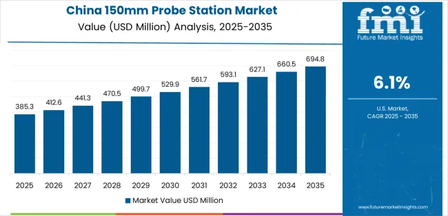
China leads the global 150mm probe station market with a 6.1% CAGR, supported by extensive semiconductor investments and manufacturing localization. National programs promoting self-sufficiency in chip production have boosted demand for advanced wafer testing systems. Domestic research centers and semiconductor companies are adopting precision probe stations for device characterization, reliability testing, and yield optimization. Partnerships between local equipment suppliers and global measurement system providers enhance production capacity and technical expertise. Rapid development of semiconductor clusters in Shanghai, Shenzhen, and Beijing strengthens infrastructure for precision instrumentation and high-accuracy wafer testing solutions.
Key Market Factors:
- Expansion of semiconductor fabrication and microelectronics research centers
- Government incentives supporting domestic probe station production
- Integration of automation and AI-driven test capabilities in laboratories
- Collaboration with global equipment manufacturers for system upgrades
How is India developing its 150mm Probe Station Market?
India’s 150mm probe station market grows at 5.6% CAGR, supported by increased semiconductor manufacturing investments and national electronics policy initiatives. The establishment of fabrication and assembly facilities under Make in India has raised demand for wafer testing and measurement equipment. Universities and R&D institutions are deploying probe stations for microdevice research and reliability testing. The entry of global test equipment suppliers through joint ventures is expanding local availability of high-precision instruments. Growth in electronics manufacturing services (EMS) and chip design firms enhances the country’s testing equipment ecosystem.
Market Development Factors:
- National semiconductor policy supporting test and measurement infrastructure
- Collaboration with global OEMs to establish local manufacturing and service centers
- Increased adoption of probe stations in academic and industrial research labs
- Expansion of EMS and chip design companies driving localized equipment demand
How is Germany strengthening the 150mm Probe Station Market?
Germany’s market grows at 5.2% CAGR, supported by advanced precision engineering and automation research. The country’s semiconductor testing ecosystem benefits from collaborations between academic institutions and equipment manufacturers. German probe station suppliers are focusing on high-resolution imaging integration and temperature-controlled platforms for accurate wafer analysis. The demand for probe stations is increasing across automotive electronics and industrial sensor testing applications. Strong industrial standards and engineering excellence sustain Germany’s position in precision measurement and semiconductor evaluation technologies.
Key Market Characteristics:
- Development of temperature-stabilized and automated wafer testing systems
- High adoption in automotive and industrial sensor evaluation
- Collaboration between universities and precision equipment manufacturers
- Continuous improvement in mechanical accuracy and software control interfaces
How is Brazil expanding its 150mm Probe Station Market?
Brazil’s market grows at 4.7% CAGR, supported by the gradual development of its electronics and semiconductor assembly industries. The expansion of testing laboratories and microelectronics education programs has driven adoption of probe stations for research and prototype verification. Partnerships between universities, government institutions, and international equipment suppliers are improving access to modern testing infrastructure. Growth in automotive and consumer electronics manufacturing also supports the use of wafer-level diagnostic systems. Local distributors are expanding after-sales support and maintenance capabilities, improving the country’s capacity for advanced semiconductor testing operations.
Market Development Factors:
- Growth of academic and industrial testing laboratories across major cities
- Expansion of electronic component assembly and R&D sectors
- Increased collaboration with global probe station suppliers for technical training
- Strengthened distribution and maintenance networks improving accessibility
How is the United States advancing its 150mm Probe Station Market?
The United States records a 4.3% CAGR, driven by innovation in semiconductor testing, research laboratories, and advanced wafer fabrication. The market benefits from strong government and private sector funding in microelectronics and nanotechnology research. Probe stations are being widely utilized for MEMS, photonics, and RF component evaluation. Equipment manufacturers are integrating AI and data analytics to enhance probe precision and repeatability. Expanding collaborations between national labs, universities, and semiconductor firms support continuous technological advancement in measurement and testing systems.
Key Market Factors:
- Growth in microelectronics and nanotechnology research applications
- Integration of AI and data analytics into testing processes
- Federal funding supporting advanced semiconductor R&D infrastructure
- Collaboration between academic institutions and commercial equipment providers
How is the United Kingdom progressing in the 150mm Probe Station Market?
The United Kingdom’s market grows at 3.8% CAGR, supported by expansion in nanotechnology research and semiconductor material development. Universities and R&D institutions are adopting advanced probe systems for device validation and material analysis. The country’s innovation-driven ecosystem supports integration of measurement automation and environmental control in laboratory testing. Collaborations between academic researchers and precision engineering companies are improving system design and calibration accuracy. Government support for semiconductor design and advanced materials research maintain steady demand for probe stations in public and private laboratories.
Market Characteristics:
- Growth in nanotechnology and material characterization research programs
- Collaboration between academia and engineering firms for system refinement
- Adoption of automation and environmental control in wafer testing
- Public funding supporting semiconductor and electronic materials R&D
How is Japan maintaining its 150mm Probe Station Market?
Japan’s market grows at 3.4% CAGR, supported by its strong foundation in precision instrumentation and electronic testing. The country’s semiconductor ecosystem continues to emphasize high-quality wafer probing for advanced device development. Domestic manufacturers are improving probe head accuracy, contact stability, and thermal management for submicron-scale measurements. Integration of automation, robotics, and optical inspection systems enhances operational consistency. Research institutions are exploring hybrid probe technologies combining electrical and optical testing methods for next-generation semiconductor applications. Japan’s long-standing focus on precision engineering ensures stable market performance despite global competition.
Market Development Factors:
- Continuous improvement in precision and reliability of probe head technologies
- Integration of robotics and optical systems in testing platforms
- Expansion of hybrid electrical-optical testing for advanced device research
- Strong institutional collaboration supporting high-accuracy instrumentation innovation
What is the competitive landscape of the 150mm Probe Station Market?
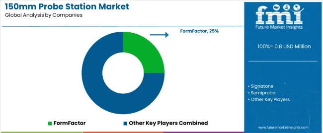
The 150mm probe station market is moderately concentrated, with a small group of specialized semiconductor equipment manufacturers competing across testing and measurement applications. FormFactor leads the market with an estimated 25.0% global share, driven by its advanced probe station designs, automation capabilities, and integration with wafer-level test systems used in semiconductor research and production. Its established relationships with major foundries and research institutions further reinforce its leadership.
Signatone and Semiprobe follow as key mid-tier competitors, offering cost-efficient and customizable probe stations suitable for academic, R&D, and low-volume industrial applications. Their competitive advantage lies in design flexibility, modular configurations, and responsive technical support for emerging testing requirements. Micromanipulator and MicroXact specialize in precision engineering, focusing on thermal and electrical stability for sensitive device measurements, particularly in power electronics and MEMS applications.
STAr Technologies and MPI Corporation provide integrated probe and test solutions that align with semiconductor process control and reliability testing needs. Both companies benefit from close collaborations with integrated device manufacturers (IDMs) and testing laboratories in Asia-Pacific, which represent major demand centers.
Competition in this segment revolves around precision, automation, and customization capabilities, as end users prioritize accurate data acquisition, reproducibility, and minimal downtime. Market growth is sustained by increased semiconductor R&D activity, miniaturization trends, and the ongoing shift toward wafer-level validation in advanced electronics manufacturing.
Key Players in the 150mm Probe Station Market
- FormFactor
- Signatone
- Semiprobe
- Micromanipulator
- MicroXact
- STAr Technologies
- MPI Corporation
Scope of the Report
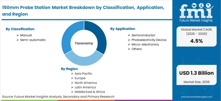
| Metric | Value |
|---|---|
| Quantitative Units | USD 0.84 Bn to USD 1.30 Bn, at a CAGR of 4.50% |
| Market Definition | 150mm probe stations are wafer-level test platforms designed to hold, position, and electrically contact 150mm (6-inch) semiconductor wafers and devices for parametric testing, failure analysis, and device characterization in semiconductor, optoelectronics, and microelectronics research and production environments. |
| Classification Segmentation | Manual, Semi-automatic |
| Application Segmentation | Semiconductor, Photoelectricity Device, Micro-electronics, Others |
| Regions Covered | North America, Latin America, Europe, East Asia, South Asia, Oceania, Middle East & Africa |
| Countries Covered | China, India, Germany, Brazil, USA, UK, Japan, and 40 plus countries |
| Key Companies Profiled | FormFactor, Signatone, Semiprobe, Micromanipulator, MicroXact, STAr Technologies, MPI Corporation |
| Forecast Period | 2026 to 2036 |
| Approach | Hybrid bottom-up and top-down modeling validated against primary research inputs and publicly available industry data. |
150mm Probe Station Market by Segments
Classification:
- Manual
- Semi-automatic
Application:
- Semiconductor
- Photoelectricity Device
- Micro-electronics
- Others
Region:
- Asia Pacific
- China
- Japan
- South Korea
- India
- Australia & New Zealand
- ASEAN
- Rest of Asia Pacific
- Europe
- Germany
- United Kingdom
- France
- Italy
- Spain
- Nordic
- BENELUX
- Rest of Europe
- North America
- United States
- Canada
- Mexico
- Latin America
- Brazil
- Chile
- Rest of Latin America
- Middle East & Africa
- Kingdom of Saudi Arabia
- Other GCC Countries
- Turkey
- South Africa
- Other African Union
- Rest of Middle East & Africa
Bibliography
- SEMI. (2024). World Fab Forecast: 150mm Wafer Fab Capacity by Device Type. SEMI.
- FormFactor Inc. (2024). Annual Report 2024: Probe Systems Division. FormFactor.
- International Electrotechnical Commission. (2024). IEC 60747: Semiconductor Devices, Test and Measurement Methods. IEC.
- USA Department of Energy. (2024). Wide Bandgap Semiconductor Technology Roadmap: SiC and GaN Device Manufacturing. DOE.
- European Commission. (2024). European Chips Act: Semiconductor Research Infrastructure Investment Framework. European Commission.
This bibliography is provided for reader reference. The full FMI report contains the complete reference list with primary research documentation.
Frequently Asked Questions
How large is the demand for 150mm Probe Station in the global market in 2026?
Demand for 150mm Probe Station in the global market is estimated to be valued at USD 0.84 billion in 2026.
What will be the market size of 150mm Probe Station by 2036?
Market size for 150mm Probe Station is projected to reach USD 1.30 billion by 2036.
What is the expected demand growth between 2026 and 2036?
Demand is expected to grow at a CAGR of 4.50% between 2026 and 2036.
Which Classification is poised to lead sales by 2026?
Manual accounts for 62.0% in 2026, reflecting its established position across primary procurement channels.
How significant is Semiconductor in driving adoption in 2026?
Semiconductor represents 34.0% of segment share, supported by procurement standardization across major end-use verticals.
What country records the fastest growth?
China is projected to grow at a CAGR of 6.10% during 2026 to 2036.
What is the projected growth for India?
India is projected to expand at a CAGR of 5.60% during 2026 to 2036.
What is included in the scope of this report?
Market scope covers manual and semi-automatic 150mm probe stations, including thermal chuck variants, RF-capable configurations, and cryogenic probe systems used for wafer-level electrical testing in semiconductor fabs, university research labs, and optoelectronics manufacturing facilities.
Table of Content
- Executive Summary
- Global Market Outlook
- Demand to side Trends
- Supply to side Trends
- Technology Roadmap Analysis
- Analysis and Recommendations
- Market Overview
- Market Coverage / Taxonomy
- Market Definition / Scope / Limitations
- Research Methodology
- Chapter Orientation
- Analytical Lens and Working Hypotheses
- Market Structure, Signals, and Trend Drivers
- Benchmarking and Cross-market Comparability
- Market Sizing, Forecasting, and Opportunity Mapping
- Research Design and Evidence Framework
- Desk Research Programme (Secondary Evidence)
- Company Annual and Sustainability Reports
- Peer-reviewed Journals and Academic Literature
- Corporate Websites, Product Literature, and Technical Notes
- Earnings Decks and Investor Briefings
- Statutory Filings and Regulatory Disclosures
- Technical White Papers and Standards Notes
- Trade Journals, Industry Magazines, and Analyst Briefs
- Conference Proceedings, Webinars, and Seminar Materials
- Government Statistics Portals and Public Data Releases
- Press Releases and Reputable Media Coverage
- Specialist Newsletters and Curated Briefings
- Sector Databases and Reference Repositories
- FMI Internal Proprietary Databases and Historical Market Datasets
- Subscription Datasets and Paid Sources
- Social Channels, Communities, and Digital Listening Inputs
- Additional Desk Sources
- Expert Input and Fieldwork (Primary Evidence)
- Primary Modes
- Qualitative Interviews and Expert Elicitation
- Quantitative Surveys and Structured Data Capture
- Blended Approach
- Why Primary Evidence is Used
- Field Techniques
- Interviews
- Surveys
- Focus Groups
- Observational and In-context Research
- Social and Community Interactions
- Stakeholder Universe Engaged
- C-suite Leaders
- Board Members
- Presidents and Vice Presidents
- R&D and Innovation Heads
- Technical Specialists
- Domain Subject-matter Experts
- Scientists
- Physicians and Other Healthcare Professionals
- Governance, Ethics, and Data Stewardship
- Research Ethics
- Data Integrity and Handling
- Primary Modes
- Tooling, Models, and Reference Databases
- Desk Research Programme (Secondary Evidence)
- Data Engineering and Model Build
- Data Acquisition and Ingestion
- Cleaning, Normalisation, and Verification
- Synthesis, Triangulation, and Analysis
- Quality Assurance and Audit Trail
- Market Background
- Market Dynamics
- Drivers
- Restraints
- Opportunity
- Trends
- Scenario Forecast
- Demand in Optimistic Scenario
- Demand in Likely Scenario
- Demand in Conservative Scenario
- Opportunity Map Analysis
- Product Life Cycle Analysis
- Supply Chain Analysis
- Investment Feasibility Matrix
- Value Chain Analysis
- PESTLE and Porter’s Analysis
- Regulatory Landscape
- Regional Parent Market Outlook
- Production and Consumption Statistics
- Import and Export Statistics
- Market Dynamics
- Global Market Analysis 2021 to 2025 and Forecast, 2026 to 2036
- Historical Market Size Value (USD Million) Analysis, 2021 to 2025
- Current and Future Market Size Value (USD Million) Projections, 2026 to 2036
- Y to o to Y Growth Trend Analysis
- Absolute $ Opportunity Analysis
- Global Market Pricing Analysis 2021 to 2025 and Forecast 2026 to 2036
- Global Market Analysis 2021 to 2025 and Forecast 2026 to 2036, By Classification
- Introduction / Key Findings
- Historical Market Size Value (USD Million) Analysis By Classification , 2021 to 2025
- Current and Future Market Size Value (USD Million) Analysis and Forecast By Classification , 2026 to 2036
- Manual
- Semi-automatic
- Manual
- Y to o to Y Growth Trend Analysis By Classification , 2021 to 2025
- Absolute $ Opportunity Analysis By Classification , 2026 to 2036
- Global Market Analysis 2021 to 2025 and Forecast 2026 to 2036, By Application
- Introduction / Key Findings
- Historical Market Size Value (USD Million) Analysis By Application, 2021 to 2025
- Current and Future Market Size Value (USD Million) Analysis and Forecast By Application, 2026 to 2036
- Semiconductor
- Photoelectricity Device
- Micro-electronics
- Others
- Semiconductor
- Y to o to Y Growth Trend Analysis By Application, 2021 to 2025
- Absolute $ Opportunity Analysis By Application, 2026 to 2036
- Global Market Analysis 2021 to 2025 and Forecast 2026 to 2036, By Region
- Introduction
- Historical Market Size Value (USD Million) Analysis By Region, 2021 to 2025
- Current Market Size Value (USD Million) Analysis and Forecast By Region, 2026 to 2036
- North America
- Latin America
- Western Europe
- Eastern Europe
- East Asia
- South Asia and Pacific
- Middle East & Africa
- Market Attractiveness Analysis By Region
- North America Market Analysis 2021 to 2025 and Forecast 2026 to 2036, By Country
- Historical Market Size Value (USD Million) Trend Analysis By Market Taxonomy, 2021 to 2025
- Market Size Value (USD Million) Forecast By Market Taxonomy, 2026 to 2036
- By Country
- USA
- Canada
- Mexico
- By Classification
- By Application
- By Country
- Market Attractiveness Analysis
- By Country
- By Classification
- By Application
- Key Takeaways
- Latin America Market Analysis 2021 to 2025 and Forecast 2026 to 2036, By Country
- Historical Market Size Value (USD Million) Trend Analysis By Market Taxonomy, 2021 to 2025
- Market Size Value (USD Million) Forecast By Market Taxonomy, 2026 to 2036
- By Country
- Brazil
- Chile
- Rest of Latin America
- By Classification
- By Application
- By Country
- Market Attractiveness Analysis
- By Country
- By Classification
- By Application
- Key Takeaways
- Western Europe Market Analysis 2021 to 2025 and Forecast 2026 to 2036, By Country
- Historical Market Size Value (USD Million) Trend Analysis By Market Taxonomy, 2021 to 2025
- Market Size Value (USD Million) Forecast By Market Taxonomy, 2026 to 2036
- By Country
- Germany
- UK
- Italy
- Spain
- France
- Nordic
- BENELUX
- Rest of Western Europe
- By Classification
- By Application
- By Country
- Market Attractiveness Analysis
- By Country
- By Classification
- By Application
- Key Takeaways
- Eastern Europe Market Analysis 2021 to 2025 and Forecast 2026 to 2036, By Country
- Historical Market Size Value (USD Million) Trend Analysis By Market Taxonomy, 2021 to 2025
- Market Size Value (USD Million) Forecast By Market Taxonomy, 2026 to 2036
- By Country
- Russia
- Poland
- Hungary
- Balkan & Baltic
- Rest of Eastern Europe
- By Classification
- By Application
- By Country
- Market Attractiveness Analysis
- By Country
- By Classification
- By Application
- Key Takeaways
- East Asia Market Analysis 2021 to 2025 and Forecast 2026 to 2036, By Country
- Historical Market Size Value (USD Million) Trend Analysis By Market Taxonomy, 2021 to 2025
- Market Size Value (USD Million) Forecast By Market Taxonomy, 2026 to 2036
- By Country
- China
- Japan
- South Korea
- By Classification
- By Application
- By Country
- Market Attractiveness Analysis
- By Country
- By Classification
- By Application
- Key Takeaways
- South Asia and Pacific Market Analysis 2021 to 2025 and Forecast 2026 to 2036, By Country
- Historical Market Size Value (USD Million) Trend Analysis By Market Taxonomy, 2021 to 2025
- Market Size Value (USD Million) Forecast By Market Taxonomy, 2026 to 2036
- By Country
- India
- ASEAN
- Australia & New Zealand
- Rest of South Asia and Pacific
- By Classification
- By Application
- By Country
- Market Attractiveness Analysis
- By Country
- By Classification
- By Application
- Key Takeaways
- Middle East & Africa Market Analysis 2021 to 2025 and Forecast 2026 to 2036, By Country
- Historical Market Size Value (USD Million) Trend Analysis By Market Taxonomy, 2021 to 2025
- Market Size Value (USD Million) Forecast By Market Taxonomy, 2026 to 2036
- By Country
- Kingdom of Saudi Arabia
- Other GCC Countries
- Turkiye
- South Africa
- Other African Union
- Rest of Middle East & Africa
- By Classification
- By Application
- By Country
- Market Attractiveness Analysis
- By Country
- By Classification
- By Application
- Key Takeaways
- Key Countries Market Analysis
- USA
- Pricing Analysis
- Market Share Analysis, 2025
- By Classification
- By Application
- Canada
- Pricing Analysis
- Market Share Analysis, 2025
- By Classification
- By Application
- Mexico
- Pricing Analysis
- Market Share Analysis, 2025
- By Classification
- By Application
- Brazil
- Pricing Analysis
- Market Share Analysis, 2025
- By Classification
- By Application
- Chile
- Pricing Analysis
- Market Share Analysis, 2025
- By Classification
- By Application
- Germany
- Pricing Analysis
- Market Share Analysis, 2025
- By Classification
- By Application
- UK
- Pricing Analysis
- Market Share Analysis, 2025
- By Classification
- By Application
- Italy
- Pricing Analysis
- Market Share Analysis, 2025
- By Classification
- By Application
- Spain
- Pricing Analysis
- Market Share Analysis, 2025
- By Classification
- By Application
- France
- Pricing Analysis
- Market Share Analysis, 2025
- By Classification
- By Application
- India
- Pricing Analysis
- Market Share Analysis, 2025
- By Classification
- By Application
- ASEAN
- Pricing Analysis
- Market Share Analysis, 2025
- By Classification
- By Application
- Australia & New Zealand
- Pricing Analysis
- Market Share Analysis, 2025
- By Classification
- By Application
- China
- Pricing Analysis
- Market Share Analysis, 2025
- By Classification
- By Application
- Japan
- Pricing Analysis
- Market Share Analysis, 2025
- By Classification
- By Application
- South Korea
- Pricing Analysis
- Market Share Analysis, 2025
- By Classification
- By Application
- Russia
- Pricing Analysis
- Market Share Analysis, 2025
- By Classification
- By Application
- Poland
- Pricing Analysis
- Market Share Analysis, 2025
- By Classification
- By Application
- Hungary
- Pricing Analysis
- Market Share Analysis, 2025
- By Classification
- By Application
- Kingdom of Saudi Arabia
- Pricing Analysis
- Market Share Analysis, 2025
- By Classification
- By Application
- Turkiye
- Pricing Analysis
- Market Share Analysis, 2025
- By Classification
- By Application
- South Africa
- Pricing Analysis
- Market Share Analysis, 2025
- By Classification
- By Application
- USA
- Market Structure Analysis
- Competition Dashboard
- Competition Benchmarking
- Market Share Analysis of Top Players
- By Regional
- By Classification
- By Application
- Competition Analysis
- Competition Deep Dive
- FormFactor
- Overview
- Product Portfolio
- Profitability by Market Segments (Product/Age /Sales Channel/Region)
- Sales Footprint
- Strategy Overview
- Marketing Strategy
- Product Strategy
- Channel Strategy
- Signatone
- Semiprobe
- Micromanipulator
- MicroXact
- STAr Technologies
- MPI Corporation
- FormFactor
- Competition Deep Dive
- Assumptions & Acronyms Used
List of Tables
- Table 1: Global Market Value (USD Million) Forecast by Region, 2021 to 2036
- Table 2: Global Market Value (USD Million) Forecast by Classification , 2021 to 2036
- Table 3: Global Market Value (USD Million) Forecast by Application, 2021 to 2036
- Table 4: North America Market Value (USD Million) Forecast by Country, 2021 to 2036
- Table 5: North America Market Value (USD Million) Forecast by Classification , 2021 to 2036
- Table 6: North America Market Value (USD Million) Forecast by Application, 2021 to 2036
- Table 7: Latin America Market Value (USD Million) Forecast by Country, 2021 to 2036
- Table 8: Latin America Market Value (USD Million) Forecast by Classification , 2021 to 2036
- Table 9: Latin America Market Value (USD Million) Forecast by Application, 2021 to 2036
- Table 10: Western Europe Market Value (USD Million) Forecast by Country, 2021 to 2036
- Table 11: Western Europe Market Value (USD Million) Forecast by Classification , 2021 to 2036
- Table 12: Western Europe Market Value (USD Million) Forecast by Application, 2021 to 2036
- Table 13: Eastern Europe Market Value (USD Million) Forecast by Country, 2021 to 2036
- Table 14: Eastern Europe Market Value (USD Million) Forecast by Classification , 2021 to 2036
- Table 15: Eastern Europe Market Value (USD Million) Forecast by Application, 2021 to 2036
- Table 16: East Asia Market Value (USD Million) Forecast by Country, 2021 to 2036
- Table 17: East Asia Market Value (USD Million) Forecast by Classification , 2021 to 2036
- Table 18: East Asia Market Value (USD Million) Forecast by Application, 2021 to 2036
- Table 19: South Asia and Pacific Market Value (USD Million) Forecast by Country, 2021 to 2036
- Table 20: South Asia and Pacific Market Value (USD Million) Forecast by Classification , 2021 to 2036
- Table 21: South Asia and Pacific Market Value (USD Million) Forecast by Application, 2021 to 2036
- Table 22: Middle East & Africa Market Value (USD Million) Forecast by Country, 2021 to 2036
- Table 23: Middle East & Africa Market Value (USD Million) Forecast by Classification , 2021 to 2036
- Table 24: Middle East & Africa Market Value (USD Million) Forecast by Application, 2021 to 2036
List of Figures
- Figure 1: Global Market Pricing Analysis
- Figure 2: Global Market Value (USD Million) Forecast 2021-2036
- Figure 3: Global Market Value Share and BPS Analysis by Classification , 2026 and 2036
- Figure 4: Global Market Y-o-Y Growth Comparison by Classification , 2026-2036
- Figure 5: Global Market Attractiveness Analysis by Classification
- Figure 6: Global Market Value Share and BPS Analysis by Application, 2026 and 2036
- Figure 7: Global Market Y-o-Y Growth Comparison by Application, 2026-2036
- Figure 8: Global Market Attractiveness Analysis by Application
- Figure 9: Global Market Value (USD Million) Share and BPS Analysis by Region, 2026 and 2036
- Figure 10: Global Market Y-o-Y Growth Comparison by Region, 2026-2036
- Figure 11: Global Market Attractiveness Analysis by Region
- Figure 12: North America Market Incremental Dollar Opportunity, 2026-2036
- Figure 13: Latin America Market Incremental Dollar Opportunity, 2026-2036
- Figure 14: Western Europe Market Incremental Dollar Opportunity, 2026-2036
- Figure 15: Eastern Europe Market Incremental Dollar Opportunity, 2026-2036
- Figure 16: East Asia Market Incremental Dollar Opportunity, 2026-2036
- Figure 17: South Asia and Pacific Market Incremental Dollar Opportunity, 2026-2036
- Figure 18: Middle East & Africa Market Incremental Dollar Opportunity, 2026-2036
- Figure 19: North America Market Value Share and BPS Analysis by Country, 2026 and 2036
- Figure 20: North America Market Value Share and BPS Analysis by Classification , 2026 and 2036
- Figure 21: North America Market Y-o-Y Growth Comparison by Classification , 2026-2036
- Figure 22: North America Market Attractiveness Analysis by Classification
- Figure 23: North America Market Value Share and BPS Analysis by Application, 2026 and 2036
- Figure 24: North America Market Y-o-Y Growth Comparison by Application, 2026-2036
- Figure 25: North America Market Attractiveness Analysis by Application
- Figure 26: Latin America Market Value Share and BPS Analysis by Country, 2026 and 2036
- Figure 27: Latin America Market Value Share and BPS Analysis by Classification , 2026 and 2036
- Figure 28: Latin America Market Y-o-Y Growth Comparison by Classification , 2026-2036
- Figure 29: Latin America Market Attractiveness Analysis by Classification
- Figure 30: Latin America Market Value Share and BPS Analysis by Application, 2026 and 2036
- Figure 31: Latin America Market Y-o-Y Growth Comparison by Application, 2026-2036
- Figure 32: Latin America Market Attractiveness Analysis by Application
- Figure 33: Western Europe Market Value Share and BPS Analysis by Country, 2026 and 2036
- Figure 34: Western Europe Market Value Share and BPS Analysis by Classification , 2026 and 2036
- Figure 35: Western Europe Market Y-o-Y Growth Comparison by Classification , 2026-2036
- Figure 36: Western Europe Market Attractiveness Analysis by Classification
- Figure 37: Western Europe Market Value Share and BPS Analysis by Application, 2026 and 2036
- Figure 38: Western Europe Market Y-o-Y Growth Comparison by Application, 2026-2036
- Figure 39: Western Europe Market Attractiveness Analysis by Application
- Figure 40: Eastern Europe Market Value Share and BPS Analysis by Country, 2026 and 2036
- Figure 41: Eastern Europe Market Value Share and BPS Analysis by Classification , 2026 and 2036
- Figure 42: Eastern Europe Market Y-o-Y Growth Comparison by Classification , 2026-2036
- Figure 43: Eastern Europe Market Attractiveness Analysis by Classification
- Figure 44: Eastern Europe Market Value Share and BPS Analysis by Application, 2026 and 2036
- Figure 45: Eastern Europe Market Y-o-Y Growth Comparison by Application, 2026-2036
- Figure 46: Eastern Europe Market Attractiveness Analysis by Application
- Figure 47: East Asia Market Value Share and BPS Analysis by Country, 2026 and 2036
- Figure 48: East Asia Market Value Share and BPS Analysis by Classification , 2026 and 2036
- Figure 49: East Asia Market Y-o-Y Growth Comparison by Classification , 2026-2036
- Figure 50: East Asia Market Attractiveness Analysis by Classification
- Figure 51: East Asia Market Value Share and BPS Analysis by Application, 2026 and 2036
- Figure 52: East Asia Market Y-o-Y Growth Comparison by Application, 2026-2036
- Figure 53: East Asia Market Attractiveness Analysis by Application
- Figure 54: South Asia and Pacific Market Value Share and BPS Analysis by Country, 2026 and 2036
- Figure 55: South Asia and Pacific Market Value Share and BPS Analysis by Classification , 2026 and 2036
- Figure 56: South Asia and Pacific Market Y-o-Y Growth Comparison by Classification , 2026-2036
- Figure 57: South Asia and Pacific Market Attractiveness Analysis by Classification
- Figure 58: South Asia and Pacific Market Value Share and BPS Analysis by Application, 2026 and 2036
- Figure 59: South Asia and Pacific Market Y-o-Y Growth Comparison by Application, 2026-2036
- Figure 60: South Asia and Pacific Market Attractiveness Analysis by Application
- Figure 61: Middle East & Africa Market Value Share and BPS Analysis by Country, 2026 and 2036
- Figure 62: Middle East & Africa Market Value Share and BPS Analysis by Classification , 2026 and 2036
- Figure 63: Middle East & Africa Market Y-o-Y Growth Comparison by Classification , 2026-2036
- Figure 64: Middle East & Africa Market Attractiveness Analysis by Classification
- Figure 65: Middle East & Africa Market Value Share and BPS Analysis by Application, 2026 and 2036
- Figure 66: Middle East & Africa Market Y-o-Y Growth Comparison by Application, 2026-2036
- Figure 67: Middle East & Africa Market Attractiveness Analysis by Application
- Figure 68: Global Market - Tier Structure Analysis
- Figure 69: Global Market - Company Share Analysis
Our Research Products

The "Full Research Suite" delivers actionable market intel, deep dives on markets or technologies, so clients act faster, cut risk, and unlock growth.

The Leaderboard benchmarks and ranks top vendors, classifying them as Established Leaders, Leading Challengers, or Disruptors & Challengers.

Locates where complements amplify value and substitutes erode it, forecasting net impact by horizon

We deliver granular, decision-grade intel: market sizing, 5-year forecasts, pricing, adoption, usage, revenue, and operational KPIs—plus competitor tracking, regulation, and value chains—across 60 countries broadly.

Spot the shifts before they hit your P&L. We track inflection points, adoption curves, pricing moves, and ecosystem plays to show where demand is heading, why it is changing, and what to do next across high-growth markets and disruptive tech

Real-time reads of user behavior. We track shifting priorities, perceptions of today’s and next-gen services, and provider experience, then pace how fast tech moves from trial to adoption, blending buyer, consumer, and channel inputs with social signals (#WhySwitch, #UX).

Partner with our analyst team to build a custom report designed around your business priorities. From analysing market trends to assessing competitors or crafting bespoke datasets, we tailor insights to your needs.
Supplier Intelligence
Discovery & Profiling
Capacity & Footprint
Performance & Risk
Compliance & Governance
Commercial Readiness
Who Supplies Whom
Scorecards & Shortlists
Playbooks & Docs
Category Intelligence
Definition & Scope
Demand & Use Cases
Cost Drivers
Market Structure
Supply Chain Map
Trade & Policy
Operating Norms
Deliverables
Buyer Intelligence
Account Basics
Spend & Scope
Procurement Model
Vendor Requirements
Terms & Policies
Entry Strategy
Pain Points & Triggers
Outputs
Pricing Analysis
Benchmarks
Trends
Should-Cost
Indexation
Landed Cost
Commercial Terms
Deliverables
Brand Analysis
Positioning & Value Prop
Share & Presence
Customer Evidence
Go-to-Market
Digital & Reputation
Compliance & Trust
KPIs & Gaps
Outputs
Full Research Suite comprises of:
Market outlook & trends analysis
Interviews & case studies
Strategic recommendations
Vendor profiles & capabilities analysis
5-year forecasts
8 regions and 60+ country-level data splits
Market segment data splits
12 months of continuous data updates
DELIVERED AS:
PDF EXCEL ONLINE

