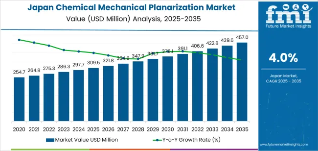
The Japan chemical mechanical planarization demand is valued at USD 309.5 million in 2025 and is forecasted to reach USD 457.0 million by 2035, reflecting a CAGR of 4.0%. Demand is driven by continued expansion of domestic semiconductor fabrication, increased utilization of advanced wafer-level processes, and growing requirements for surface-planarization precision in logic, memory, and power device production.
Adoption of smaller technology nodes, higher layer counts, and more complex device architectures further elevates the need for reliable planarity control across fabrication lines. CMP consumables represent the leading segment as fabs depend heavily on high-performance slurries, polishing pads, conditioners, and cleaning chemistries to meet strict uniformity, dishing, and defect-reduction standards. Continuous improvements in slurry formulations, pad durability, and process-specific consumable designs support throughput gains and tighter tolerance control across copper, dielectric, and tungsten CMP applications.
Kyushu & Okinawa, Kanto, and Kinki record the highest utilization levels due to their concentration of semiconductor manufacturing clusters, wafer-fabrication facilities, and precision-equipment suppliers. These regions maintain well-established supply ecosystems, specialized cleanroom manufacturing environments, and strong infrastructure supporting advanced semiconductor production. Key suppliers include Applied Materials Inc., Ebara Corporation, Lapmaster Wolters, Cabot Microelectronics (CMC Materials), and Fujimi Incorporated. These companies provide CMP tools, consumables, process-control systems, and customized planarization solutions used in semiconductor manufacturing and wafer-polishing workflows.
Early growth in Japan’s chemical-mechanical-planarization (CMP) segment is shaped by semiconductor-fabrication demand, steady equipment upgrades, and predictable consumables usage across wafer-processing lines. The early phase shows firm expansion as domestic fabs invest in process-node transitions and maintain high utilization rates for integrated-circuit production. CMP pads, slurries, conditioners, and endpoint-control systems experience stable procurement because they are essential consumables tied to each wafer cycle. This creates a consistent early-stage curve with limited volatility.
Late-stage growth continues but follows a more moderated slope as CMP demand aligns with mature fab capacity and established production workflows. Incremental process refinements, such as improved selectivity and defect-reduction slurries, support continued adoption, though gains become narrower as technology platforms stabilize. Late growth also reflects replacement cycles rather than new-capacity surges, which softens the curve compared with the early expansion phase.
Comparing both periods, the early phase benefits from active investment cycles, process-node advancements, and rising wafer starts, while the late phase reflects a mature operational environment focused on optimization rather than rapid scale-up. The overall pattern shows strong early momentum followed by controlled, incremental late-period growth within Japan’s semiconductor-manufacturing ecosystem.
| Metric | Value |
|---|---|
| Japan Chemical Mechanical Planarization Sales Value (2025) | USD 309.5 million |
| Japan Chemical Mechanical Planarization Forecast Value (2035) | USD 457.0 million |
| Japan Chemical Mechanical Planarization Forecast CAGR (2025-2035) | 4.0% |
Demand for chemical mechanical planarization in Japan is increasing because semiconductor manufacturers require precise surface-flattening processes to support advanced chip architectures used in memory, processors and power devices. CMP is essential for multi-layer interconnects, wafer thinning and defect reduction, all of which align with Japan’s focus on high-performance electronics, automotive semiconductors and specialty materials. Domestic fabs and equipment suppliers invest in new CMP slurries, pads and endpoint-control systems to meet tighter planarization tolerances as device geometries shrink.
Growth in applications such as electric vehicles, 5G devices and industrial automation strengthens the need for reliable CMP steps in both logic and memory production. Collaborations between chipmakers and materials companies further increase demand for customized CMP consumables tailored to Japanese manufacturing lines. Constraints include high cost of CMP consumables, complex slurry-waste management requirements and the need for skilled engineers to manage process stability. Smaller facilities may struggle with integration of new CMP tools due to equipment expense and cleanroom restrictions. Supply fluctuations in specialty chemicals can also affect production schedules.
Demand for chemical mechanical planarization (CMP) in Japan reflects the country’s established semiconductor fabrication base and requirements for achieving uniform surface finishing across advanced device structures. CMP supports multilayer integration, defect reduction, and planarization accuracy essential in logic, memory, and specialty device production. Japanese fabs use structured workflows combining consumables, polishing systems, and endpoint control technologies adapted to process nodes and material stacks.
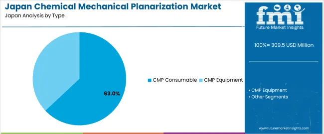
CMP consumables represent 63.0%, forming the largest category due to continuous replacement cycles and high-volume usage across semiconductor polishing steps. This group includes slurries, pads, conditioners, and cleaning solutions required for oxide, metal, and dielectric planarization. CMP equipment represents 37.0%, covering polishing tools, pad conditioning units, and endpoint monitoring systems used in 300 mm and 200 mm fabrication lines. The distribution reflects Japan’s mature fabs, where equipment lifecycles extend through upgrades, while consumables incur steady demand. Requirements are influenced by device miniaturization, surface defect control, and integration of advanced dielectric materials. Consumable selection remains central to polishing uniformity and wafer-to-wafer consistency.
Key points:
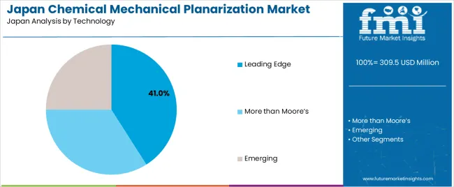
Leading-edge CMP represents 41.0%, reflecting use in advanced logic and memory processes requiring nanometer-level precision. These workflows support tight dimensional tolerances and complex multi-level copper and dielectric integration. More-than-Moore technologies account for 34.0%, covering power devices, RF components, sensors, and specialized substrates common in Japan’s mixed-device production landscape.
Emerging technologies represent 25.0%, including CMP adapted for new materials, heterogeneous integration, and packaging-related surface preparation. Technology distribution demonstrates Japan’s balanced dependence on advanced semiconductor nodes and specialty processes, with varied CMP needs driven by material hardness, surface topology, and required removal characteristics across device categories.
Key points:
Growth of advanced semiconductor manufacturing in domestic fabs, increased investment in logic and memory node transitions and rising demand for ultra-flat wafers in equipment clusters are driving demand.
In Japan, CMP consumption expands as domestic fabs in regions such as Kumamoto, Hokkaido and Ibaraki increase capacity for advanced semiconductor processes. Joint projects involving global chipmakers and Japanese firms accelerate migration toward finer logic and memory nodes, which require tighter planarization control. Japan’s strong presence in specialty materials, including slurries, pads and consumables, supports close integration between fabs and suppliers. Equipment clusters in Kyushu and the Kanto region rely on CMP to achieve uniform wafer surfaces for lithography, deposition and etching steps, reinforcing continuous demand across production cycles.
High capital cost for tool upgrades, uneven adoption among legacy-line operators and limited availability of skilled CMP process engineers restrain growth.
CMP tools require significant investment, and many Japanese fabs operating mature 200 mm lines delay upgrades due to lower margins and long equipment lifecycles. Legacy device producers may continue using older planarization protocols if node transitions are not economically justified. Japan also experiences shortages of semiconductor process engineers, particularly specialists in CMP optimization, which can slow pilot-line validation and reduce adoption of next-generation consumables. These economic and workforce constraints result in uneven uptake across different fab types.
Shift toward CMP tailored for 3D packaging, increased use of low-defect slurry systems and expansion of localized material supply define key trends.
Japanese semiconductor manufacturers are scaling CMP solutions that support 3D packaging, including TSV and advanced wafer-level packaging processes used in high-performance computing and automotive electronics. Local suppliers are developing low-defect slurries and long-life pads to improve line yield and reduce consumable cost per wafer. Fabs in Japan are strengthening domestic sourcing of key CMP materials to reduce dependence on overseas shipments and enhance supply stability, particularly for advanced oxide and metal CMP steps. These trends point to continued alignment between Japan’s semiconductor roadmap and the evolution of CMP demand.
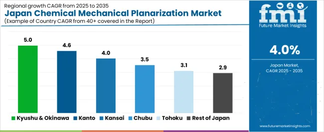
Demand for chemical mechanical planarization (CMP) in Japan is increasing as semiconductor fabs, materials suppliers, and equipment integrators expand precision polishing operations to support advanced chip production. Growth varies across regions based on wafer-fabrication density, access to specialty chemical suppliers, and ongoing investments in CMP slurries, pads, conditioners, and process-control systems. Kyushu & Okinawa leads at 5.0%, followed by Kanto (4.6%), Kinki (4.0%), Chubu (3.5%), Tohoku (3.1%), and Rest of Japan (2.9%).
| Region | CAGR (2025-2035) |
|---|---|
| Kyushu & Okinawa | 5.0% |
| Kanto | 4.6% |
| Kinki | 4.0% |
| Chubu | 3.5% |
| Tohoku | 3.1% |
| Rest of Japan | 2.9% |
Kyushu & Okinawa grows at 5.0% CAGR, supported by strong semiconductor fabrication activity centered around Kumamoto, where major expansion projects increase the need for CMP consumables and equipment. Wafer-fabrication facilities integrate advanced planarization steps to support logic, memory, and sensor production. Local suppliers distribute CMP slurries, pads, and post-CMP cleaning materials to meet production-cycle requirements. University-linked semiconductor research centers in Fukuoka collaborate with manufacturers on optimization of planarization parameters for new device architectures. Regional infrastructure supports stable chemical logistics for high-volume CMP operations, while training programs expand technical capacity for process-control and polishing-equipment operation.
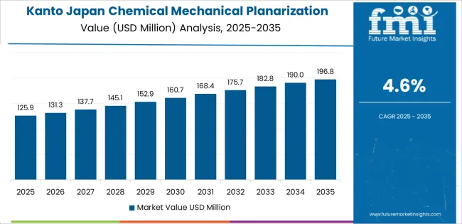
Kanto grows at 4.6% CAGR, driven by dense semiconductor supply-chain activity and a strong base of materials manufacturers across Tokyo, Kanagawa, and Saitama. CMP chemical suppliers in the region produce slurries and post-polish cleaning agents used in advanced process nodes. Research institutions in Tokyo maintain partnerships with semiconductor firms to refine planarization chemistries, improve defect control, and support next-generation wafer structures. Equipment integrators in Kanto deliver polishing platforms and metrology tools to fabs nationwide. Urban manufacturing districts show steady investment in semiconductor process optimization, raising the need for consistent CMP-grade materials.
Kinki grows at 4.0% CAGR, with semiconductor equipment suppliers and materials firms concentrated across Osaka, Kyoto, and Hyogo. Specialty-chemical companies produce CMP slurries tailored for dielectric, metal, and barrier-layer polishing. Kyoto’s research ecosystem contributes to CMP process studies, including scratch reduction, slurry-performance testing, and pad-surface analysis. Manufacturers supporting microelectronics packaging also rely on planarization steps, increasing local demand for consumables. Regional semiconductor suppliers maintain stable logistics networks connecting materials producers with fabrication facilities across Japan.
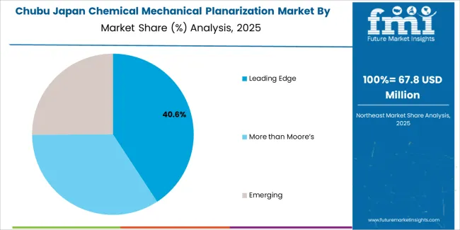
Chubu grows at 3.5% CAGR, shaped by precision-manufacturing clusters around Aichi, Shizuoka, and Nagano that use CMP consumables for semiconductor, automotive electronics, and sensor production. Local firms provide precision polishing materials and support services for wafer-level processes. Semiconductor suppliers in Nagano maintain capabilities for distributing CMP pads, slurries, and conditioning equipment to customers across central Japan. Manufacturing companies involved in electronic-component fabrication adopt advanced planarization steps to achieve required surface tolerances. Technical institutes in the region participate in applied research on polishing uniformity and surface-defect management.
Tohoku grows at 3.1% CAGR, supported by semiconductor-related facilities and materials producers across Miyagi, Fukushima, and Iwate. The region hosts electronics facilities using CMP steps for sensor, memory, and automotive-grade semiconductor components. Local companies distribute polishing consumables to meet fabrication-cycle requirements. Public research centers in Sendai participate in microfabrication research involving surface-planarization studies. Logistics networks maintain reliable access to CMP chemicals and pads for regional manufacturers.
Rest of Japan grows at 2.9% CAGR, supported by smaller semiconductor-related companies, electronics manufacturers, and materials suppliers that use CMP consumables for precision fabrication. Local firms adopt planarization in workflows for sensors, optical components, and compact semiconductor devices. Regional suppliers distribute CMP pads, slurries, conditioners, and post-CMP cleaning materials to meet production requirements. Engineering institutes participate in research on polishing uniformity and defect management.
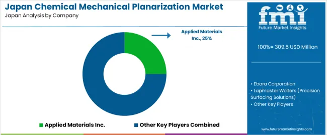
Demand for chemical mechanical planarization in Japan is shaped by semiconductor-equipment manufacturers and consumables suppliers serving integrated-device manufacturers and advanced wafer-fabrication sites. Applied Materials Inc. holds an estimated 25.0% share, supported by controlled CMP-tool performance, stable process uniformity, and long-standing adoption across leading Japanese fabs. Its platforms provide consistent removal-rate control and reliable integration with advanced-node processes.
Ebara Corporation maintains strong domestic participation with CMP systems used in 300-mm wafer lines. Its tools offer dependable platen stability and controlled slurry-distribution behaviour, supporting predictable across-wafer planarity in logic and memory production. Lapmaster Wolters (Precision Surfacing Solutions) contributes capability in precision-surface-finishing equipment used in selected Japanese process lines, emphasizing uniform material removal and durable machine construction.
Cabot Microelectronics (CMC Materials) plays a major role in consumables, supplying slurries and polishing pads with reliable particle-size control and stable chemical performance. Its materials support oxide, metal, and dielectric CMP steps across Japanese fabs. Fujimi Incorporated, a key domestic slurry supplier, provides high-purity abrasives and CMP formulations with consistent dispersion stability and verified compatibility with advanced-node requirements.
Competition in Japan centers on removal-rate uniformity, defect minimization, consumable consistency, integration with fab process flows, and local technical-support availability. Demand remains steady as Japanese semiconductor producers expand advanced logic, power devices, and memory fabrication, requiring CMP systems and consumables that deliver reproducible planarity and low-defect surfaces across increasingly complex device architectures.
| Items | Values |
|---|---|
| Quantitative Units | USD million |
| Type | CMP Consumable, CMP Equipment |
| Technology | Leading Edge, More than Moore’s, Emerging |
| Application | Integrated Circuits, Compound Semiconductors, MEMS and NEMS, Optics |
| Regions Covered | Kyushu & Okinawa, Kanto, Kinki, Chubu, Tohoku, Rest of Japan |
| Key Companies Profiled | Applied Materials Inc., Ebara Corporation, Lapmaster Wolters (Precision Surfacing Solutions), Cabot Microelectronics (CMC Materials), Fujimi Incorporated |
| Additional Attributes | Dollar sales by CMP equipment and consumables categories; adoption trends across leading-edge, More-than-Moore, and emerging semiconductor technologies; regional semiconductor manufacturing concentration across Kyushu & Okinawa, Kanto, Kinki, Chubu, Tohoku, and Rest of Japan; demand driven by wafer scaling, 3D device structures, compound semiconductor growth, and high-precision optics; competitive landscape of slurry providers, pad manufacturers, and CMP equipment suppliers in Japan. |
The demand for chemical mechanical planarization in Japan is estimated to be valued at USD 309.5 million in 2025.
The market size for the chemical mechanical planarization in Japan is projected to reach USD 457.0 million by 2035.
The demand for chemical mechanical planarization in Japan is expected to grow at a 4.0% CAGR between 2025 and 2035.
The key product types in chemical mechanical planarization in Japan are cmp consumable and cmp equipment.
In terms of technology, leading edge segment is expected to command 41.0% share in the chemical mechanical planarization in Japan in 2025.
Our Research Products

The "Full Research Suite" delivers actionable market intel, deep dives on markets or technologies, so clients act faster, cut risk, and unlock growth.

The Leaderboard benchmarks and ranks top vendors, classifying them as Established Leaders, Leading Challengers, or Disruptors & Challengers.

Locates where complements amplify value and substitutes erode it, forecasting net impact by horizon

We deliver granular, decision-grade intel: market sizing, 5-year forecasts, pricing, adoption, usage, revenue, and operational KPIs—plus competitor tracking, regulation, and value chains—across 60 countries broadly.

Spot the shifts before they hit your P&L. We track inflection points, adoption curves, pricing moves, and ecosystem plays to show where demand is heading, why it is changing, and what to do next across high-growth markets and disruptive tech

Real-time reads of user behavior. We track shifting priorities, perceptions of today’s and next-gen services, and provider experience, then pace how fast tech moves from trial to adoption, blending buyer, consumer, and channel inputs with social signals (#WhySwitch, #UX).

Partner with our analyst team to build a custom report designed around your business priorities. From analysing market trends to assessing competitors or crafting bespoke datasets, we tailor insights to your needs.
Supplier Intelligence
Discovery & Profiling
Capacity & Footprint
Performance & Risk
Compliance & Governance
Commercial Readiness
Who Supplies Whom
Scorecards & Shortlists
Playbooks & Docs
Category Intelligence
Definition & Scope
Demand & Use Cases
Cost Drivers
Market Structure
Supply Chain Map
Trade & Policy
Operating Norms
Deliverables
Buyer Intelligence
Account Basics
Spend & Scope
Procurement Model
Vendor Requirements
Terms & Policies
Entry Strategy
Pain Points & Triggers
Outputs
Pricing Analysis
Benchmarks
Trends
Should-Cost
Indexation
Landed Cost
Commercial Terms
Deliverables
Brand Analysis
Positioning & Value Prop
Share & Presence
Customer Evidence
Go-to-Market
Digital & Reputation
Compliance & Trust
KPIs & Gaps
Outputs
Full Research Suite comprises of:
Market outlook & trends analysis
Interviews & case studies
Strategic recommendations
Vendor profiles & capabilities analysis
5-year forecasts
8 regions and 60+ country-level data splits
Market segment data splits
12 months of continuous data updates
DELIVERED AS:
PDF EXCEL ONLINE
Chemical Mechanical Planarization Market Growth – Size & Forecast 2025 to 2035
Japan Aluminum Chemicals Market Report – Trends, Demand & Industry Outlook 2025-2035
Chemical Hydraulic Valves Market Size and Share Forecast Outlook 2025 to 2035
Japan Faith-based Tourism Market Size and Share Forecast Outlook 2025 to 2035
Japan Sports Tourism Market Size and Share Forecast Outlook 2025 to 2035
Chemical Vapor Deposition Market Forecast Outlook 2025 to 2035
Chemical Recycling Service Market Forecast Outlook 2025 to 2035
Chemical Dosing Equipment Market Size and Share Forecast Outlook 2025 to 2035
Chemical Filling System Market Size and Share Forecast Outlook 2025 to 2035
Japan Respiratory Inhaler Devices Market Size and Share Forecast Outlook 2025 to 2035
Japan Halal Tourism Market Size and Share Forecast Outlook 2025 to 2035
Chemical Absorbent Pads Market Size and Share Forecast Outlook 2025 to 2035
Chemical Indicator Inks Market Size and Share Forecast Outlook 2025 to 2035
Chemical Boiler Market Size and Share Forecast Outlook 2025 to 2035
Chemical Hardener Compounds Market Size and Share Forecast Outlook 2025 to 2035
Chemical Anchors Market Size and Share Forecast Outlook 2025 to 2035
Mechanical Shaft Seal Market Size and Share Forecast Outlook 2025 to 2035
Mechanical And Electronic Fuzes Market Size and Share Forecast Outlook 2025 to 2035
Chemical Peel Market Size and Share Forecast Outlook 2025 to 2035
Japan Automated People Mover Industry Size and Share Forecast Outlook 2025 to 2035

Thank you!
You will receive an email from our Business Development Manager. Please be sure to check your SPAM/JUNK folder too.
Chat With
MaRIA