Photomask Inspection Market Size and Share Forecast Outlook 2025 to 2035
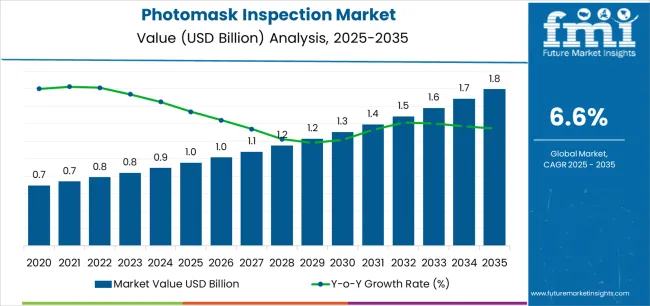
The Photomask Inspection Market is estimated to be valued at USD 1.0 billion in 2025 and is projected to reach USD 1.8 billion by 2035, registering a compound annual growth rate (CAGR) of 6.6% over the forecast period.
The photomask inspection market is expanding steadily due to increasing demand for advanced semiconductor devices and rising complexity in integrated circuit designs. Growth is being driven by rapid technological evolution in lithography, miniaturization trends, and the need for high-precision quality control in chip manufacturing.
The market is witnessing consistent adoption of automated and high-resolution inspection systems that ensure defect-free photomasks used in semiconductor fabrication. Current dynamics are influenced by the surge in foundry activities, particularly in Asia-Pacific, and ongoing investments by major semiconductor manufacturers to improve yield rates and process reliability.
Future growth is expected to be supported by the introduction of next-generation semiconductor nodes, where stringent inspection standards are essential to maintain production efficiency The overall market trajectory is underpinned by increasing capital expenditure in the semiconductor ecosystem, growing emphasis on accuracy and throughput, and continuous innovation in optical and e-beam inspection technologies aimed at ensuring superior pattern fidelity and process stability across global manufacturing facilities.
Quick Stats for Photomask Inspection Market
- Photomask Inspection Market Industry Value (2025): USD 1.0 billion
- Photomask Inspection Market Forecast Value (2035): USD 1.8 billion
- Photomask Inspection Market Forecast CAGR: 6.6%
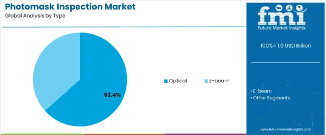
- Leading Segment in Photomask Inspection Market in 2025: Optical (63.4%)
- Key Growth Region in Photomask Inspection Market: North America, Asia-Pacific, Europe
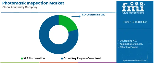
- Top Key Players in Photomask Inspection Market: KLA Corporation, SML Holding N.V., Applied Materials, Inc., Camtek Ltd., Carl Zeiss AG, Hermes Microvision Inc., Hitachi High-Tech Corporation, JEOL Ltd., Lasertec Corporation, Nanometrics Incorporated, Nikon Corporation, NuFlare Technology Inc., Onto Innovation Inc., Photronics, Inc., Toppan Photomasks, Inc.

| Metric |
Value |
| Photomask Inspection Market Estimated Value in (2025 E) |
USD 1.0 billion |
| Photomask Inspection Market Forecast Value in (2035 F) |
USD 1.8 billion |
| Forecast CAGR (2025 to 2035) |
6.6% |
Segmental Analysis
The market is segmented by Type and Application and region. By Type, the market is divided into Optical and E-beam. In terms of Application, the market is classified into Foundries and IDMs. Regionally, the market is classified into North America, Latin America, Western Europe, Eastern Europe, Balkan & Baltic Countries, Russia & Belarus, Central Asia, East Asia, South Asia & Pacific, and the Middle East & Africa.
Insights into the Type Segment

The optical segment, holding 63.40% of the type category, has been dominating the market due to its cost efficiency, fast throughput, and effectiveness in detecting surface and pattern defects during photomask production. Its leadership is supported by widespread use in semiconductor fabrication lines, where real-time defect analysis and corrective feedback are critical for maintaining production quality.
Advancements in optical imaging resolution and automated data analytics have further enhanced accuracy and reduced false defect detection rates. The segment’s adoption is being reinforced by integration with AI-based defect classification systems, improving operational precision and decision-making speed.
Continued innovations in wavelength optimization and inspection algorithms are expected to sustain optical inspection as the preferred choice for mainstream applications, ensuring consistent market dominance even as e-beam systems gain traction for next-generation semiconductor nodes.
Insights into the Application Segment

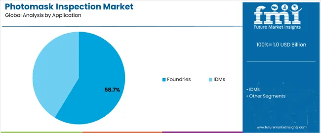
The foundries segment, representing 58.70% of the application category, has remained the leading application area due to its extensive use of photomask inspection in high-volume semiconductor production. Demand from foundries has been driven by increasing adoption of advanced process nodes, where precision and defect control are critical for maintaining yield and device reliability.
Strategic investments in manufacturing infrastructure and automation have amplified inspection requirements, ensuring high throughput and minimal downtime. The segment’s growth is further supported by collaborations between equipment suppliers and foundry operators to develop application-specific inspection solutions tailored to complex design geometries.
As foundries continue to scale production for advanced chips used in consumer electronics, automotive, and data center applications, photomask inspection systems are expected to remain integral to quality assurance processes, securing the segment’s dominant position in the global market landscape.
Photomask Inspection Market Overview
- Growing demand for photomask inspection in the semiconductor industry.
- Photomask inspection is a critical step in the semiconductor manufacturing process that ensures high-quality production.
- Increasing demand for semiconductors in various industries, such as automotive, healthcare, and consumer electronics, the photomask inspection market is experiencing a surge in demand.
- Constant advancements in technology.
- As the semiconductor industry continues to innovate and develop new and more complex devices, the need for accurate and reliable photomask inspection becomes more critical.
- The market is witnessing an increase in demand for advanced photomask inspection techniques, such as optical and electron beam inspection, which can detect defects at a much smaller scale.
- Rise of artificial intelligence and machine learning is also driving the growth of the photomask inspection market. AI-powered photomask inspection systems can analyze vast amounts of data quickly and accurately, improving the detection rate of defects.
- Increasing demand for larger and more complex photomasks.
- The trend towards miniaturization in the semiconductor industry has LED to the development of smaller and more complex devices, which require larger and more intricate photomasks.
- Trend is expected to continue, driving the demand for photomask inspection systems that can handle larger and more complex photomasks.
Key Opportunities in the Photomask Inspection Market
- Development of more advanced inspection technologies. Traditional inspection methods rely on optical inspection, which is limited in its ability to detect defects at the nanoscale level. Manufacturers that can develop more advanced inspection technologies, such as electron beam inspection, will have a significant competitive advantage in the market.
- The photomask inspection market is poised for significant growth in the coming years as semiconductor manufacturers continue to push the boundaries of technology.
- Photomask inspection is a critical step in the semiconductor manufacturing process, as it ensures that the masks used to create the tiny circuits on computer chips are free from defects.
- As more advanced chips are developed, the demand for high-quality photomask inspection solutions will only increase.
- Growing trend of outsourcing photomask inspection services.
- Many semiconductor manufacturers are looking to outsource their photomask inspection needs to third-party providers, which can help to reduce costs and improve efficiency.
- Manufacturers that can offer high-quality photomask inspection services at a competitive price point will be well-positioned to take advantage of this trend.
Challenges in the Photomask Inspection Market
- As the semiconductor industry moves towards smaller geometries and more advanced designs, the photomasks used in the manufacturing process are becoming increasingly complex. Complexity makes it more difficult for inspection equipment to accurately identify defects and errors in the photomasks, which can lead to lower yields and higher costs.
- Rising demand for high-speed and high-resolution inspection equipment restricts market growth.
- As semiconductor manufacturing becomes more advanced, the need for faster and more precise inspection equipment is growing. This is putting pressure on manufacturers to develop new and innovative inspection technologies to meet these evolving demands.
- The high cost of developing and manufacturing photomask inspection equipment is limiting the number of companies that can effectively compete in the market.
- High costs lead to consolidation among equipment manufacturers, which reduces competition and potentially leads to higher prices for customers.
Photomask Inspection Industry Analysis by Top Investment Segments
In Terms of Type, the Optical Segment Leads the Market Growth
| Attributes |
Details |
| Top Type |
Optical |
| CAGR (2025 to 2035) |
6.7% |
- High precision and accuracy offered by optical inspection systems are expected to drive the segment’s growth.
- These systems use advanced imaging technology to detect defects in photomasks, which are used in the semiconductor manufacturing process.
- The optical segment is expected to continue to dominate the market due to the growing demand for high-performance semiconductors and the need for precision manufacturing processes.
- Optical inspection systems are cost-effective and offer high throughput, making them ideal for high-volume manufacturing, which is further increased their popularity in the market.
In terms of Application, the IDMs Segment is dominating the Market
| Attributes |
Details |
| Top Application |
IDMs |
| CAGR (2025 to 2035) |
6.4% |
- IDMs are responsible for the majority of semiconductor manufacturing. As a result, they have a higher demand for photomask inspection systems compared to other segments of the market.
- IDMs have a higher budget for research and development, allowing them to invest in advanced technologies and inspection systems which further increases the demand for photomask inspection systems in the IDMs segment.
- Increasing demand for high-performance semiconductors and the need for precision manufacturing processes will further drive the growth of the segment in the market.
Analysis of Top Countries Engaged in Manufacturing, Distributing, and Using Photomask Inspection Solutions
| Countries |
CAGR (2025 to 2035) |
| United States |
7.0% |
| United Kingdom |
7.6% |
| China |
7.4% |
| Japan |
8.0% |
| South Korea |
8.7% |
Growing Semiconductor Industry in the United States
- Growing semiconductor industry in the country.
- The United States has a significant presence in the semiconductor industry, with many leading semiconductor companies based in the country, which resulted in the demand for advanced photomask inspection systems that can detect defects at the nanoscale level and ensure high-quality output.
- Increasing demand for advanced electronic devices such as smartphones and laptops is driving the growth of the semiconductor industry in the country, further increasing the demand for photomask inspection systems.
The United Kingdom Has a Strong Presence in Industries Such as Aerospace, Defense, and Automotive
- Growing demand for advanced semiconductors in various industries such as automotive, aerospace, and defense.
- The country has a strong presence in these industries and is focused on developing advanced technologies that require high-performance semiconductors, which resulted in the demand for advanced photomask inspection systems that can ensure the quality of the semiconductors used in these industries.
Government Investing Heavily in the Semiconductor Business in China
- China is one of the largest consumers of semiconductors in the world, with a rapidly growing domestic semiconductor industry.
- This has resulted in the demand for advanced photomask inspection systems that can detect defects and ensure high-quality output.
- The Chinese government is investing heavily in the semiconductor industry, driving the growth of the industry in the country and increasing the demand for photomask inspection systems.
Surge in Demand for Advanced Photomask Inspection Systems in Japan
- The strong presence of leading semiconductor companies such as Toshiba, Fujitsu, and Renesas.
- Increased focus of leading semiconductor companies in developing advanced semiconductors for various applications such as automotive, healthcare, and industrial automation has LED to a surge in demand for advanced photomask inspection systems in Japan.
- The semiconductor industry in Japan is increasingly relying on these systems to ensure the quality of the semiconductors used in these applications. As a result, the demand for high-performance photomask inspection systems is growing in the market.
Companies in South Korea are Heavily Investing in Developing Advanced Semiconductors
- Companies in South Korea are heavily investing in developing advanced semiconductors for various applications, such as smartphones, laptops, and other electronic devices.
- Increasing demand for such devices leads to a surge in demand for photomask inspection systems that can effectively ensure the quality of the semiconductors used in these devices.
- Rising demand for photomask inspection machines in South Korea can be attributed to various factors such as the government's support for the semiconductor industry, the highly skilled workforce, and the increasing complexity of semiconductor chips.
- As the demand for advanced semiconductors continues to rise, the photomask inspection market is expected to grow further, presenting new opportunities for local companies to innovate and expand their business.
Competitive Landscape of the Photomask Inspection Market

The market is highly competitive, with several key players dominating the industry. Companies are constantly innovating and introducing new technologies to gain a competitive edge over their rivals. They are also focusing on offering customized solutions to meet the specific needs of their clients.
Moreover, partnerships and collaborations with other companies and research organizations are becoming increasingly important in this market. The key players are also investing heavily in research and development activities to develop advanced photomask inspection technologies that offer high accuracy, speed, and reliability.
Recent Developments in the Photomask Inspection Market
- In 2024, in an effort to bolster its standing in the photomask inspection market and broaden its range of offerings, KLA Corporation acquired Orbotech. Orbotech is a top provider of optical inspection and metrology solutions and specializes in the development of high-resolution imaging and AI-powered defect detection capabilities for advanced photomask inspection systems. KLA aims to leverage these capabilities to help semiconductor and display industries improve yield and reduce manufacturing costs.
- In 2025, Applied Materials, a leading semiconductor equipment manufacturer, introduced a new line of chip-making equipment and an accompanying AI system. This latest offering includes a suite of products designed to improve the efficiency and performance of chip manufacturing processes. In addition to the hardware, the AI system incorporates advanced machine learning algorithms to analyze data in real time and optimize the performance of the equipment.
Leading Companies in the Photomask Inspection Market
- SML Holding N.V.
- Applied Materials, Inc.
- Camtek Ltd.
- Carl Zeiss AG
- Hermes Microvision Inc.
- Hitachi High-Tech Corporation
- JEOL Ltd.
- KLA Corporation
- Lasertec Corporation
- Nanometrics Incorporated
- Nikon Corporation
- NuFlare Technology Inc.
- Onto Innovation Inc.
- Photronics, Inc.
- Toppan Photomasks, Inc.
Key Coverage in the Photomask Inspection Market Report
- Mask Inspection Equipment Market Landscape
- Photomask Printing Industry Assessment
- High-End Photomask Inspection System Market Overview
- Photomask Equipment Pricing Outlook
- Photomasks Supplier Analysis
Top Segments Studied in the Photomask Inspection Market
By Type:
By Application:
By Region:
- North America
- Latin America
- East Asia
- South Asia
- Europe
- Oceania
- MEA
Frequently Asked Questions
How big is the photomask inspection market in 2025?
The global photomask inspection market is estimated to be valued at USD 1.0 billion in 2025.
What will be the size of photomask inspection market in 2035?
The market size for the photomask inspection market is projected to reach USD 1.8 billion by 2035.
How much will be the photomask inspection market growth between 2025 and 2035?
The photomask inspection market is expected to grow at a 6.6% CAGR between 2025 and 2035.
What are the key product types in the photomask inspection market?
The key product types in photomask inspection market are optical and e-beam.
Which application segment to contribute significant share in the photomask inspection market in 2025?
In terms of application, foundries segment to command 58.7% share in the photomask inspection market in 2025.
