- Market Size (2026)
- USD 7.2 Bn
- Forecast (2036)
- USD 12.3 Bn
- CAGR (2026 to 2036)
- 5.5%
How big is Semiconductor Encapsulants Market in 2026?
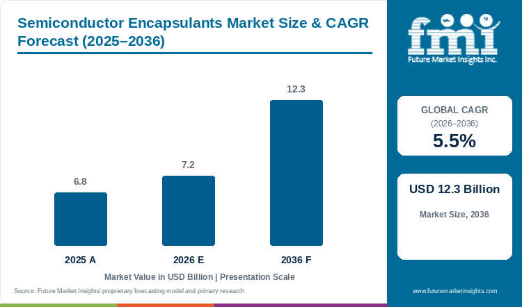
Global semiconductor encapsulants sales record USD 6.8 Billion in 2025, are estimated to advance to USD 7.2 Billion in 2026, and are projected toward USD 12.3 Billion by 2036 under a 5.5% CAGR.
Preventing substrate warpage and moisture-induced interfacial delamination across fine-pitch chiplet interposers requires thermoset compounds with high spherical silica loadings, positioning epoxy molding compounds to account for an estimated 39.7% of material type demand in 2026. Future Market Insights projects semiconductor encapsulants expenditure to expand from a 2025 valuation of USD 6.8 Billion to an expected USD 7.2 Billion in 2026 and a predicted USD 12.3 Billion by 2036, reflecting an anticipated 5.5% CAGR and USD 5.1 Billion in added annual sales. Outsourced assembly plants are accelerating adoption of low-stress compression resins alongside semiconductor packaging materials, corroborated by February 2026 Semiconductor Industry Association data showing that global semiconductor sales jumped 25.6% to a record USD 791.7 billion in 2025 as logic sales surged 39.9% to USD 301.9 billion and memory rose 34.8% to USD 223.1 billion [1]. Nonetheless, capillary flow resistance inside sub-15-micron copper-pillar standoffs and tight refining capacity for synthetic ultra-low-alpha spherical silica still restrain qualification speed.
Key Market Trends & Insights
- By material type: Epoxy molding compounds are projected to command 39.7% in 2026 through sub-ppm ionic chloride purity and low thermal expansion coefficients.
- By packaging application: IC packages are estimated to garner 31.9% in 2026 due to high-volume DRAM memory stack and logic die overmolding across Asian OSAT plants.
- By cure technology: Thermal cure chemistries are slated to retain 40.4% in 2026 via predictable gel-time kinetics in automated multi-cavity chase molds.
- By end use: Consumer electronics is projected to deliver 39.1% in 2026 as smartphone RF front-end modules and wearable system-in-package designs demand ultra-thin protection.
Regional Highlights
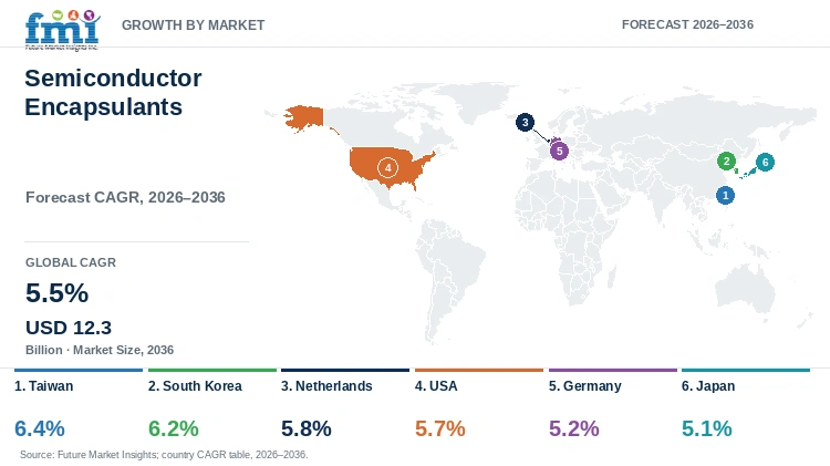
- Fastest national expansion: Taiwan is projected to head major semiconductor manufacturing hubs with a 6.4% compound growth rate through 2036 via CoWoS 2.5D interposer and fan-out capacity additions.
- Regional foundry trajectory: South Korean encapsulant consumption is expected to rise 6.2% annually ahead of Dutch fabs at 5.8% and American lines at 5.7%, whereas German fabs are forecast to record 5.2% above Japanese output at 5.1%.
Market Size & Forecast
Table 1: Market Size and Forecast for the Semiconductor Encapsulants Market (USD billion and CAGR percentage), 2025 to 2036
| Metric | Value |
|---|---|
| 2025 Market Size | USD 6.8 Billion |
| Estimated Market Size in 2026 | USD 7.2 Billion |
| Projected Market Size by 2036 | USD 12.3 Billion |
| CAGR, 2026 to 2036 | 5.5% |
| Added Revenue, 2026 to 2036 | USD 5.1 Billion |
Outsourced semiconductor assembly and test facilities confront severe interfacial delamination and solder-bump fatigue as power densities rise across automotive and AI packages. In August 2025, a reliability review published in Polymers documented that epoxy underfill composites require fused-silica filler loadings up to 70 weight percent to bridge the thermal expansion mismatch between silicon dies at 2.5 to 2.8 ppm per degree Celsius and organic FR4 substrates at 18 to 24 ppm per degree Celsius [2]. Consequently, packaging engineers are replacing conventional transfer-molded pellets with vacuum-assisted molded underfill material that fills sub-20-micron flip-chip standoffs without micro-voids. Transitioning toward granular and sheet compression resins stabilizes reconstituted 300-millimeter wafers during post-mold cure.
Wafer-Level Encapsulation Throughput and Consumption Sizing
Table 2: Wafer-Level Encapsulation Throughput and Material Consumption Indicators for the Semiconductor Encapsulants Market (USD Billion and operational ranges), 2025 to 2036
| Metric | 2025 | 2026 | 2036 |
|---|---|---|---|
| Market size (USD Billion) | 6.8 | 7.2 | 12.3 |
| Global encapsulant resin & compound volume (kilotons) | 310 to 345 | 328 to 365 | 510 to 575 |
| Spherical fused-silica filler loading range (wt%) | 82% to 88% | 84% to 89% | 86% to 92% |
| Average advanced-package material spend per wafer (USD) | 42.0 to 68.0 | 45.0 to 74.0 | 65.0 to 110.0 |
Operational note: Volume ranges reflect global consumption of epoxy molding compounds and liquid underfills across IDM and OSAT lines normalized to 300-millimeter wafer equivalents.
Multi-die chiplet architectures require sub-micron spherical silica cuts with alpha-particle emissions below 0.001 counts per hour per square centimeter to prevent soft memory errors. Chemical formulators coordinate silane coupling treatments with spherical silica refiners to maintain low melt viscosity at filler loadings approaching 90 weight percent.
OSAT & Foundry Packaging Line Expenditure Sizing
Table 3: OSAT & Foundry Packaging Facility Expenditure Indicators for the Semiconductor Encapsulants Market (USD), 2025 to 2036
| Metric | 2025 | 2026 | 2036 |
|---|---|---|---|
| Active global OSAT & IDM back-end facilities | 1,180 | 1,220 | 1,560 |
| Average annual encapsulant procurement per facility (USD million) | 5.8 | 5.9 | 7.9 |
| Standard leadframe EMC price band (USD per kg) | 12.0 to 22.0 | 13.0 to 24.0 | 16.0 to 30.0 |
| High-purity chiplet liquid & film underfill price band (USD per kg) | 140.0 to 320.0 | 150.0 to 345.0 | 210.0 to 460.0 |
Table 4: Segment Revenue Indicators for the Semiconductor Encapsulants Market (USD Billion and percentages), 2026
| Metric | Value | Institutional Reference Basis |
|---|---|---|
| Market size, 2026 | USD 7.2 Billion | 2026 global packaging materials baseline |
| Thermal cure system revenue, 2026 | USD 2.9 Billion | 40.4% cure technology allocation |
| Epoxy molding compounds revenue, 2026 | USD 2.9 Billion | 39.7% material type allocation |
| Consumer electronics end-use revenue, 2026 | USD 2.8 Billion | 39.1% end-use segment allocation |
High-density packaging lines depend on tight spiral-flow viscosity control to fill narrow copper-pillar standoffs without sweeping delicate bond wires. Assembly engineering directors benchmark encapsulant formulations alongside die-attach adhesives to verify JEDEC Moisture Sensitivity Level 1 survival across 260-degree lead-free reflow profiles.
Analyst Perspective
"Back-end packaging engineers now specify ultra-low-alpha nano-silica fillers and halogen-free biphenyl resins for 2.5D chiplet interposers and 800-volt silicon carbide modules. Severe wafer warpage and fine-pitch capillary voiding still require extensive thermal-shock qualification before foundries approve new formulations."
- Nikhil Kaitwade, Principal Consultant, Future Market Insights.
How is the semiconductor encapsulants market segmented?
The semiconductor encapsulants market is segmented by material type, packaging application, cure technology, and end use. In 2026, epoxy molding compounds are projected at 39.7%, IC packages at 31.9%, thermal cure at 40.4%, and consumer electronics at 39.1%.
By material type: Epoxy Molding Compounds, Liquid Encapsulants, Silicone Encapsulants, and Underfill Materials.
By packaging application: IC Packages, Power Modules, LED Packages, and Advanced Packaging.
By cure technology: Thermal Cure, UV Cure, Dual Cure, and Room-Temperature Cure.
By end use: Consumer Electronics, Automotive Electronics, Industrial Electronics, and Telecommunications.
Why do epoxy molding compounds lead the material type category?
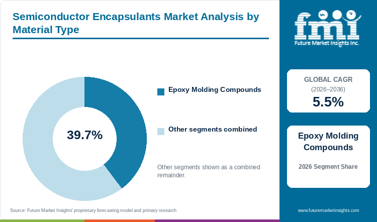
Epoxy molding compounds are projected to command 39.7% of the material type segment in 2026, aided by wafer compression overmolding.
Table 5: Material Type Share for the Semiconductor Encapsulants Market (percentage share), 2026
| Material Type | Share (2026) |
|---|---|
| Epoxy Molding Compounds | 39.7% |
| Other Segments Combined | 60.3%* |
| Total | 100.0% |
*Note: Silicone encapsulants together with specialty potting resins represent the balance of 2026 demand.
Table 6: Material Type Leadership and Market Growth for the Semiconductor Encapsulants Market (segment and CAGR percentage), 2026 to 2036
| Metric | Value |
|---|---|
| Global CAGR (2026 to 2036) | 5.5% |
| Leading Segment | Epoxy Molding Compounds |
High-silica thermoset preforms and granular resins anchor semiconductor overmolding because they match the thermal expansion coefficient of silicon dies across multi-cavity transfer presses. Foundries pair low-warpage granular molding compounds with fast-flow board level underfill material to protect micro-bump arrays against solder joint fatigue.
- Epoxy molding compounds are projected to command 39.7% of material type demand in 2026 through sub-ppm extractable chloride purity and high moisture barrier performance.
- Sumitomo Bakelite Co., Ltd. announced new production lines in Suzhou and Singapore in October 2026 to double SUMIKON EME mold underfill capacity and triple compression-molding granule output [3].
What drives IC packages to the forefront of the packaging application segment?
IC packages are estimated to garner 31.9% of packaging application revenue in 2026, benefiting from memory stack and logic encapsulation.
Memory stacks and logic processors consume the largest tonnage of molding compounds because global electronics supply chains manufacture billions of leadframe and substrate units annually. While quad flat no-lead packages rely on transfer molding, memory foundries are scaling semiconductor packaging lines that laminate non-conductive films and sheet encapsulants across High Bandwidth Memory cubes.
- IC packages are estimated to comprise 31.9% of packaging application spending in 2026 as Asian OSAT facilities expand DDR5 and AI logic overmolding throughput.
- An April 2025 packaging review published in Micromachines documented how 2.5D and 3D chip packages including TSMC CoWoS and Samsung HBM require warpage control below 2 microns per 20 millimeters across interconnect densities reaching 10,000 to 1,000,000 I/O per square centimeter [4].
How does thermal cure maintain its 40.4% share in the cure technology segment?
Thermal cure chemistries are slated to retain 40.4% of cure technology demand in 2026, accompanied by cross-linking beneath silicon dies.
Heat-activated anhydride and phenolic hardeners dominate back-end assembly lines because thermal cross-linking cures shadowed resin zones beneath metal heat spreaders and stacked silicon dies where UV light cannot penetrate. Process engineers tune latent catalyst kinetics inside automated chase molds alongside die bonder equipment to achieve void-free gelation.
- Thermal cure is anticipated to constitute 40.4% of cure technology revenue in 2026 due to predictable post-mold cure shrinkage and high glass-transition stability.
- Nagase ChemteX Corporation updated technical specifications in August 2025 for its Liquid Molding Compound and advanced-Sheet Molding Compound systems operating at 4 MPa compression pressure and a 10-minute 125-degree in-mold thermal cure followed by a 60-minute 150-degree post-mold cure [5].
What positions consumer electronics as the leading end use category in 2026?
Consumer electronics applications are anticipated to contribute 39.1% of end use consumption in 2026, anchored by smartphone processor module protection.
Annual replacement cycles across 5G smartphones and ultra-thin portable computers generate continuous base-load consumption of fine-filler molding compounds. Radio-frequency front-end modules combine low-dielectric epoxy overmolding with conformal EMI shielding to prevent signal crosstalk across tightly packed system-in-package substrates.
- Consumer electronics is forecast to hold 39.1% of end use sales in 2026 as mobile application processors and wearable sensors require ultra-thin package profiles.
- A December 2025 University of Texas at Dallas study in the Journal of Neural Engineering demonstrated that PECVD amorphous silicon carbide encapsulation achieves -80.5 MPa compressive stress and 8.0 to 15.6 teraohm insulation resistance under accelerated voltage aging [6].
What are the drivers, restraints, and opportunities in the semiconductor encapsulants market?
Across the semiconductor encapsulants market, 2.5D AI chiplet and 800-volt SiC power module scaling is projected to accelerate specialty resin demand whereas ultra-low-alpha silica bottlenecks restrict supply and panel-level compression molding expands margins.
- Driver: Rapid capacity additions in 2.5D CoWoS AI accelerators and 800-volt automotive silicon carbide traction inverters compel OSATs to specify high-Tg low-warpage encapsulants.
- Restraint: Capillary flow resistance below 15-micron bump pitches and concentrated refining capacity for synthetic ultra-low-alpha spherical silica inflate formulation costs.
- Opportunity: Granular and film-assisted vacuum compression molding resins alongside alumina-filled high-thermal-conductivity compounds capture premium foundry qualifications.
Growth Analysis and Future Potential: Chiplet Interposers and SiC Power Packaging Catalysts
Scaling heterogeneous chiplet processors and wide-bandgap automotive power modules is converting specialty semiconductor encapsulants into critical yield determinants across global assembly plants. Foundries are replacing standard ortho-cresol novolac epoxies with multi-functional biphenyl and dicyclopentadiene resin networks that resist delamination above 200 degrees Celsius. According to FMI, rising electric-vehicle inverter voltages also expand demand for high-dielectric silicon carbide module overmolding and silicone gel potting. In May 2026, the Semiconductor Industry Association reported that Q1 2026 global semiconductor sales rose 25% quarter-over-quarter to USD 298.5 billion while March 2026 monthly sales jumped 79.2% year-over-year to USD 99.5 billion [7]. Qualifying low-warpage compression compounds secures multi-year foundry supply allocations.
Risk Assessment and Operational Hurdles: Sub-Micron Filler Bottlenecks and Fine-Pitch Voiding
Rheological flow resistance in sub-15-micron copper-pillar standoffs and raw-material bottlenecks in ultra-low-alpha spherical silica constrain encapsulant supply growth. When flip-chip bump pitches narrow below 15 microns, conventional capillary underfills suffer filler filtration and micro-voiding that trigger solder-bump bridging during thermal shock. In March 2026, the European Chemicals Agency advanced REACH committee evaluations on per- and polyfluoroalkyl substances alongside April 2026 EU PFHxA restrictions impacting microelectronic fluoropolymers and surfactants [8]. Meanwhile, formulators supplying electronic sealants and chiplet underfills depend on a small group of Japanese synthetic silica refiners, creating lead-time volatility during fab ramp-ups.
Commercial Opportunity Analysis: Film-Assisted Compression Molding and Alumina-Filled Thermal Resins
Electronic chemical formulators capture high gross margins by commercializing sheet-type vacuum compression compounds and spherical-alumina-filled thermal resins. Conventional transfer molding exerts fluid drag that sweeps fragile gold and copper wires, whereas film-assisted vacuum compression molding encapsulates 600-millimeter reconstituted panels without wire deformation. In October 2026, SEMI projected that global 300-millimeter fab equipment spending will rise 31% year-over-year to USD 149 billion in 2026 and total USD 227 billion in 2029 as 38 new 300-millimeter fabs begin construction across 2026 and 2027 [9]. Pairing alumina-filled potting compound systems with thermal interface materials enables suppliers to capture next-generation EV powertrain and AI server qualifications.
Semiconductor Encapsulants Market by Country (2026 to 2036)
According to FMI, Taiwanese OSAT and foundry consumption is projected to post a leading 6.4% ten-year compound rate through 2036, while Japanese domestic resin demand is expected to increase at 5.1% annually. Commercial performance across East Asian foundry clusters alongside European and North American semiconductor corridors depends on localizing cleanroom resin compounding near advanced foundries and supporting customer device qualification under AEC-Q101 for discrete semiconductors and AEC-Q100 Grade 0 (-40 to +150 degrees Celsius ambient) for automotive integrated circuits.
Table 7: Country CAGR and Primary Growth Levers for the Semiconductor Encapsulants Market (CAGR percentage and operational drivers), 2026 to 2036
| Country | CAGR (2026 to 2036) | Primary Growth Lever |
|---|---|---|
| Taiwan | 6.4% | CoWoS 2.5D interposer compression molding and panel-level fan-out OSAT capacity expansions |
| South Korea | 6.2% | HBM3e and HBM4 memory stack molded underfill and non-conductive film qualification |
| Netherlands | 5.8% | Automotive radar, photonic integrated circuit, and power semiconductor packaging lines |
| USA | 5.7% | CHIPS Act advanced packaging fab construction and defense microelectronics encapsulation |
| Germany | 5.2% | 800-volt silicon carbide traction inverter overmolding in Saxony and Bavaria fabs |
| Japan | 5.1% | Ultra-low-alpha spherical silica refinement and synthetic biphenyl epoxy export production |
Source: Future Market Insights analysis
Taiwan Semiconductor Encapsulants Market Outlook (2026 to 2036)
Unlike IDM-led Western semiconductor markets, Taiwan concentrates global consumption of wafer-level granular and sheet compression resins inside pure-play foundry and OSAT clusters across Hsinchu and Kaohsiung. In June 2025, a joint study by National Kaohsiung University of Science and Technology and Advanced Semiconductor Engineering in Kaohsiung published in Computers Materials & Continua proved that 19 kPa vacuum molding and plasma contact angles below 50 degrees minimize flip-chip molded underfill voids [10]. Taiwanese semiconductor encapsulants consumption is projected to compound at a 6.4% rate through 2036 alongside fan-out panel-level packaging investments. Because domestic lines rely on imported ultra-low-alpha spherical silica, global formulators are commissioning local cleanroom compounding hubs in Kaohsiung.
Key takeaway: In Taiwan, rapid 2.5D CoWoS and fan-out panel-level capacity expansions are projected to drive premier global demand for low-warpage granular and sheet compression encapsulants.
South Korea Semiconductor Encapsulants Market Outlook (2026 to 2036)
South Korean semiconductor encapsulants procurement is expected to grow at a 6.2% compound pace through 2036 across Pyeongtaek and Icheon packaging fabs. Whereas Taiwan focuses on logic interposers, South Korea's material demand is uniquely dominated by 12-high and 16-high High Bandwidth Memory vertical DRAM stacking. In June 2026, Resonac Holdings Corporation confirmed that the Japan Patent Office upheld Patent No. 7687499 on controlled-modulus liquid encapsulants for 2.5D generative AI and HBM packages as 2.5D packaging expands at an 18.8% CAGR through 2031 [11]. Compressing vertical DRAM cubes into tight Z-height envelopes creates severe heat-flux and micro-bump voiding risks, prompting Korean memory makers to qualify fluxing non-conductive films and high-conductivity molded underfills.
Key takeaway: In South Korea, 12-high and 16-high High Bandwidth Memory production ramps are expected to anchor high-margin procurement of thermally conductive molded underfills.
Netherlands Semiconductor Encapsulants Market Outlook (2026 to 2036)
What sets the Netherlands apart from high-volume Asian memory hubs is its specialization in panel-based advanced equipment metrology, optically coupled photonic integrated circuits, and 77-gigahertz automotive radar transceivers. In October 2026, SEMI recognized the Nordson SonoFlex acoustic inspection platform with the 2026 Best of West Award for scanning panel-based semiconductor assemblies 2x faster and isolating sub-micron encapsulation voids up to 8x faster [12]. Dutch semiconductor encapsulants demand is anticipated to progress at a 5.8% compound annual rate through 2036 as optical transceiver and automotive sensor lines scale production across Eindhoven and Nijmegen. Because European REACH rules restrict fluorinated surfactants, formulators supply PFAS-free optically transparent UV-curable liquid encapsulants and halogen-free biphenyl pellets.
Key takeaway: In the Netherlands, photonic integrated circuit assembly and REACH halogen-free rules are forecast to steer buyers toward PFAS-free UV-curable and low-stress epoxy encapsulants.
USA Semiconductor Encapsulants Market Outlook (2026 to 2036)
Unlike Asian commercial OSAT hubs, United States encapsulant demand is uniquely shaped by radiation-hardened aerospace defense microelectronics alongside federal strategic investments in 300-millimeter foundry and 2.5D packaging lines. In October 2026, the Semiconductor Industry Association applauded GlobalFoundries' USD 21 billion expansion across two new 300-millimeter fabs in Malta, New York adding 900,000 wafers per year per fab under the U.S.-Japan Strategic Investment Initiative [13]. United States semiconductor encapsulants shipments are anticipated to progress at a 5.7% compound pace through 2036 as new packaging fabs ramp across New York and Arizona alongside Texas corridors. To overcome lengthy defense qualification cycles, resin suppliers co-locate application testing labs near domestic foundry clusters.
Key takeaway: In the USA, federal 300-millimeter foundry expansions and defense microelectronics programs are anticipated to drive domestic qualification of high-reliability liquid and compression encapsulants.
Germany Semiconductor Encapsulants Market Outlook (2026 to 2036)
German semiconductor encapsulants procurement is predicted to climb at a 5.2% compound annual rate through 2036 across Silicon Saxony and Bavarian assembly plants. Unlike consumer-electronics-driven Asian packaging markets, Germany's consumption centers on 800-volt automotive silicon carbide traction inverters and high-reliability compute modules requiring customer qualification across -65 to +150 degrees Celsius thermal-cycling regimes. In January 2025, Duesseldorf-headquartered Henkel Adhesive Technologies detailed how its LOCTITE ECCOBOND UF 9000AE capillary underfill developed across 34 Duesseldorf labs fills large AI and automotive chip gaps 30% faster while surviving -65 to +150 degrees Celsius thermal cycling [14]. Because SiC junction temperatures above 200 degrees Celsius delaminate standard novolac epoxies, suppliers formulate cycloaliphatic high-Tg transfer molding resins and phenyl-silicone gels.
Key takeaway: In Germany, 800-volt automotive silicon carbide traction inverters and -65 to +150 degrees Celsius device thermal-cycling requirements are predicted to drive procurement of high-Tg molding compounds and silicone gels.
Japan Semiconductor Encapsulants Market Outlook (2026 to 2036)
Whereas other semiconductor nations are net importers of packaging chemicals, Japan occupies a unique global position as the upstream production hub for synthetic ultra-low-alpha spherical silica and panel-level organic interposer materials. In September 2025, Resonac Holdings Corporation launched the 27-member JOINT3 consortium in Yuki City, Ibaraki alongside NAMICS and TOWA to operate a 515 by 510 millimeter panel-level organic interposer prototype line [15]. Japanese domestic encapsulant sales are estimated to advance at a 5.1% compound rate over the decade ending 2036 as chemical leaders commercialize panel-level molding sheets. To offset mature domestic leadframe tonnage, Japanese formulators in Kawasaki and Yokkaichi prioritize high-margin granular compression compounds and non-conductive films.
Key takeaway: In Japan, upstream dominance in ultra-low-alpha spherical silica and the 27-member JOINT3 panel-level consortium are estimated to sustain continuous innovation in wafer and panel molding resins.
Full report country CAGRs cover: North America; Latin America; Western Europe; Eastern Europe; East Asia; South Asia and Pacific; Middle East and Africa.
Who are the notable companies in the semiconductor encapsulants market?
Sumitomo Bakelite Co., Ltd., Resonac Holdings Corporation, Henkel AG & Co. KGaA, Shin-Etsu Chemical Co., Ltd., Kyocera Corporation, Nagase ChemteX Corporation, Panasonic Holdings Corporation (Electronic Materials), and H.B. Fuller Company are the notable companies in the semiconductor encapsulants market.
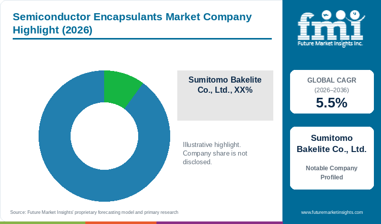
Future Market Insights notes that commercial competition splits between upstream Japanese thermoset resin producers and international liquid underfill formulators. Japanese chemical groups control upstream biphenyl resin synthesis and spherical silica silane treatment to lead transfer and compression molding compounds. International adhesive and silicone specialists lead in jettable capillary underfills and high-voltage dielectric gels.
- Epoxy Molding & Compression Resin Leaders: Sumitomo Bakelite Co., Ltd. and Resonac Holdings Corporation alongside Kyocera Corporation and Panasonic Holdings Corporation lead in high-silica transfer pellets and wafer-level granular compounds.
- Liquid Underfill & Advanced Adhesive Specialists: Henkel AG & Co. KGaA and Nagase ChemteX Corporation together with H.B. Fuller Company engineer jettable capillary underfills alongside non-conductive films and liquid compression resins.
- High-Purity Silicone & Dielectric Gel Platforms: Shin-Etsu Chemical Co., Ltd. supplies phenyl and fluorosilicone gels alongside silicone-modified molding compounds for automotive power modules.
Competitive Benchmarking: Semiconductor Encapsulants Market
Table 8: Competitive Benchmarking for the Semiconductor Encapsulants Market (qualitative capability ratings), 2026
| Company | Epoxy Molding Compound Breadth | Advanced Chiplet & Underfill Depth | Automotive Power Module Qualification | Geographic Reach |
|---|---|---|---|---|
| Sumitomo Bakelite Co., Ltd. | High | High | High | High |
| Resonac Holdings Corporation | High | High | High | High |
| Henkel AG & Co. KGaA | Medium | High | High | High |
| Shin-Etsu Chemical Co., Ltd. | Medium | High | High | High |
| Kyocera Corporation | High | High | Medium | Medium |
| Nagase ChemteX Corporation | Medium | High | Medium | Medium |
| Panasonic Holdings Corporation (Electronic Materials) | High | High | Medium | High |
| H.B. Fuller Company | Medium | High | Medium | High |
Scoring basis: Benchmark ratings evaluate commercial catalog depth across transfer molding pellets and granular compression resins alongside non-conductive films validated on 2.5D CoWoS and HBM lines. Automotive and geographic scores reflect material adoption in discrete power devices qualified under AEC-Q101 and automotive ICs qualified up to AEC-Q100 Grade 0 (-40 to +150 degrees Celsius) alongside multi-region cleanroom compounding.
Key Developments in the Semiconductor Encapsulants Market
- Sumitomo Bakelite Co., Ltd. announced a 30% production capacity expansion in June 2026 for SUMIKON EME semiconductor encapsulation materials at its 60,000-square-meter Suzhou plant serving generative AI GPU and memory packages alongside EV power devices [16].
- Resonac Holdings Corporation received the 2025 TSMC Excellent Performance Award in December 2025 for Excellence in Technology Development and Production Support across advanced packaging materials [17].
- Kyocera Corporation commercialized its flexible Sheet EMC for panel-level packaging (PLP) and wafer-level packaging (WLP) in April 2025, enabling vacuum laminator sealing that minimizes large-panel warpage and resin flow defects [18].
Key Players in the Semiconductor Encapsulants Market
Epoxy Molding & Compression Resin Leaders
- Sumitomo Bakelite Co., Ltd.
- Resonac Holdings Corporation
- Kyocera Corporation
- Panasonic Holdings Corporation (Electronic Materials)
Liquid Underfill & Advanced Adhesive Specialists
- Henkel AG & Co. KGaA
- Nagase ChemteX Corporation
- H.B. Fuller Company
High-Purity Silicone & Dielectric Gel Platforms
- Shin-Etsu Chemical Co., Ltd.
Semiconductor Encapsulants Market - Report Scope
Table 9: Report Scope for the Semiconductor Encapsulants Market (coverage fields and definitions), 2026 to 2036
| Coverage field | Report scope |
|---|---|
| Market breakdown | Material Type; Packaging Application; Cure Technology; End Use |
| Quantitative Units | USD Billion |
| Market Definition | Includes manufacturer revenue from epoxy molding compounds, liquid encapsulants, silicone dielectric gels, and capillary, non-conductive film, or molded underfills used in semiconductor and power module packaging. Category Scope Note: Excludes bare metallic leadframes, organic laminate substrates, and automated dispensing or molding press machinery. |
| Regions Covered | North America; Latin America; Western Europe; Eastern Europe; East Asia; South Asia and Pacific; Middle East and Africa |
| Countries Covered | Taiwan, South Korea, Netherlands, USA, Germany, Japan, and additional countries in the full report |
| Key Companies Covered | Sumitomo Bakelite Co., Ltd., Resonac Holdings Corporation, Henkel AG & Co. KGaA, Shin-Etsu Chemical Co., Ltd., Kyocera Corporation, Nagase ChemteX Corporation, Panasonic Holdings Corporation (Electronic Materials), H.B. Fuller Company |
| Forecast Period | 2026 to 2036 |
| Approach | Primary and secondary research with top-down and bottom-up market triangulation. |
Semiconductor Encapsulants Market - Research Methodology
Table 10: Research Methodology for the Semiconductor Encapsulants Market (research methods and approach), 2026 edition
| Method | Approach |
|---|---|
| Primary Research | Structured interviews with electronic chemical formulators, synthetic spherical silica refiners, OSAT packaging directors, and foundry qualification engineers to validate gram consumption per wafer and price bands. |
| Secondary Research | Review of corporate annual filings, SIA global sales databases, SEMI 300mm fab equipment projections, ECHA PFAS restriction dossiers, and peer-reviewed packaging journals. |
| Market Sizing and Forecasting | Top-down global semiconductor packaging material budgets reconciled against bottom-up 300-millimeter wafer starts, CoWoS/HBM stack counts, and EV power module volumes from 2026 to 2036. |
| Country Forecasting Model | National projections weight OSAT and foundry capital expenditure, High Bandwidth Memory stacking capacity, automotive SiC inverter production, and CHIPS/METI packaging subsidies across six core hubs. |
| Operational Benchmark Traceability | Resin tonnage, spherical silica weight-percent loadings, and per-wafer material spend in Tables 2, 3, and 4 trace to SIA revenue statistics, Polymers underfill reviews, and Micromachines 2.5D/3D packaging benchmarks. |
| Data Triangulation and Validation | Supplier chemical revenues are cross-checked against OSAT mold press consumption and spherical silica refinery shipments without double counting organic substrate or die-attach paste sales. |
Semiconductor Encapsulants Market by Segments
Semiconductor Encapsulants Market segmented by Material Type:
- Epoxy Molding Compounds
- Liquid Encapsulants
- Silicone Encapsulants
- Underfill Materials
Semiconductor Encapsulants Market segmented by Packaging Application:
- IC Packages
- Power Modules
- LED Packages
- Advanced Packaging
Semiconductor Encapsulants Market segmented by Cure Technology:
- Thermal Cure
- UV Cure
- Dual Cure
- Room-Temperature Cure
Semiconductor Encapsulants Market segmented by End Use:
- Consumer Electronics
- Automotive Electronics
- Industrial Electronics
- Telecommunications
Semiconductor Encapsulants Market by Region
- North America
- United States
- Canada
- Latin America
- Brazil
- Mexico
- Argentina
- Chile
- Western Europe
- Germany
- France
- United Kingdom
- Italy
- Spain
- Benelux
- Nordics
- Eastern Europe
- Poland
- Czech Republic
- Romania
- Hungary
- East Asia
- China
- Japan
- South Korea
- South Asia and Pacific
- India
- ASEAN
- Australia and New Zealand
- Middle East and Africa
- GCC Countries
- South Africa
- Türkiye
- Israel
Research Sources and Bibliography
- [1] Semiconductor Industry Association. (2026, February 6). Global Annual Semiconductor Sales Increase 25.6% to $791.7 Billion in 2025. Semiconductor Industry Association (SIA).
- [2] Plachy, Z., Prazanova, A., Dusek, K., & Geczy, A. (2025, August 13). Underfill: A Review of Reliability Improvement Methods in Electronics Production. Polymers, 17(16), 2206 (PubMed Central PMCID PMC12389694).
- [3] Sumitomo Bakelite Co., Ltd. (2026, October 9). Expansion of Production Capacity for Advanced Semiconductor Encapsulation Materials in Suzhou, China, and Singapore. Sumitomo Bakelite Information & Telecommunication Materials Division.
- [4] Chen, G., Wang, G., Wang, Z., & Wang, L. (2025, April 2). Electronic Chip Package and Co-Packaged Optics (CPO) Technology for Modern AI Era: A Review. Micromachines, 16(4), 431 (MDPI).
- [5] Nagase ChemteX Corporation. (2025, August 4). LMC | Nagase Chemtex Co., Ltd. Nagase ChemteX Corporation.
- [6] Nguyen, C. K., Geramifard, N., Wu, Y., Bhatt, M., Joshi-Imre, A., Negi, S., & Cogan, S. F. (2025, December 30). Electrical characterization and accelerated aging of amorphous silicon carbide implantable encapsulation. Journal of Neural Engineering, 22(6), 066040 (PubMed PMID 41467780).
- [7] Semiconductor Industry Association. (2026, May 4). Global Semiconductor Sales Increase 25% from Q4 2025 to Q1 2026. Semiconductor Industry Association (SIA).
- [8] European Chemicals Agency. (2026, March 26). Per- and polyfluoroalkyl substances (PFAS) - ECHA. European Chemicals Agency (ECHA).
- [9] SEMI. (2026, October 13). Global 300mm Fab Equipment Spending to Reach $227 Billion in 2029 as Buildout Accelerates, SEMI Projects. SEMI.
- [10] Hu, I., Hung, T.-C., Zhou, M.-H., Lin, H.-S., & Chen, D.-L. (2025, June 9). Void Formation Analysis in the Molded Underfill Process for Flip-Chip Packaging. Computers, Materials & Continua, 84(1), 537-551 (Tech Science Press).
- [11] Resonac Holdings Corporation. (2026, June 17). Resonac's Patent on Liquid Encapsulant for AI Semiconductor Packages Upheld. Resonac News Releases.
- [12] SEMI. (2026, October 15). Nordson SonoFlex Acoustic System Wins 2026 Best of West Award. SEMI.
- [13] Semiconductor Industry Association. (2026, October 14). SIA Applauds GlobalFoundries Expansion Under U.S.-Japan Initiative. Semiconductor Industry Association (SIA).
- [14] Henkel AG & Co. KGaA. (2025, January 15). High-tech underfill solutions open up new design possibilities for computer chips. Henkel Adhesive Technologies (Duesseldorf, Germany).
- [15] Resonac Holdings Corporation. (2025, September 3). Resonac Launches 27-Member "JOINT3" Consortium to Develop Next-Generation Semiconductor Packaging. Resonac News Releases.
- [16] Sumitomo Bakelite Co., Ltd. (2026, June 25). Expansion of Production Capacity for Semiconductor Encapsulation Materials at Sumitomo Bakelite (Suzhou) Co., Ltd. Sumitomo Bakelite Information & Telecommunication Materials Division.
- [17] Resonac Holdings Corporation. (2025, December 1). Resonac Receives "2025 TSMC Excellent Performance Award". Resonac News Releases.
- [18] Kyocera Corporation. (2025, April 10). Sheet EMC for PLP/WLP | Epoxy Molding Compounds for Semiconductors | KYOCERA. Kyocera Corporation Chemical Products Division.
- [19] Resonac Holdings Corporation. (2026, April 20). Resonac Launches R&D Center for Next-Gen Semiconductor Package Technology under U.S.-Japanese Consortium "US-JOINT". Resonac News Releases.
This bibliography is provided for reader reference and is not exhaustive. The full report contains the complete reference list and detailed citations.
This Report Answers
- How large is the semiconductor encapsulants market in 2026 and what is forecast for 2036?
- Which 2.5D chiplet and silicon carbide power module pressures support demand for semiconductor encapsulants?
- Why do epoxy molding compounds lead the material type category?
- Why does thermal cure lead the cure technology category globally?
- How do material growth rates differ across Taiwan, South Korea, the Netherlands, the USA, Germany, and Japan?
- Which leading chemical companies supply semiconductor molding compounds and liquid underfills today?
- What limits adoption or supplier switching in the semiconductor encapsulants market?
- What should packaging engineers evaluate before qualifying a semiconductor encapsulant?
Frequently Asked Questions
How big is the semiconductor encapsulants market in 2026, and what is forecast for 2036?
Global semiconductor encapsulants consumption is estimated to total USD 7.2 Billion in 2026 after recording USD 6.8 Billion in 2025, and FMI forecasts the sector toward USD 12.3 Billion by 2036 on advanced chiplet and power module demand.
What is the CAGR for the semiconductor encapsulants market from 2026 to 2036?
Future Market Insights projects a 5.5% compound annual growth rate from 2026 through 2036, representing an expected USD 5.1 Billion increase in annual material sales between 2026 and 2036 across OSAT and foundry packaging lines.
Which material type segment leads the semiconductor encapsulants market?
Epoxy molding compounds are projected to command 39.7% of material type revenue in 2026 because high spherical silica loadings match silicon thermal expansion during transfer and compression molding.
Which cure technology segment leads the semiconductor encapsulants market?
Thermal cure systems are expected to account for 40.4% of cure technology demand in 2026 through complete polymer cross-linking beneath opaque silicon dies and stable 260-degree reflow performance.
Which country has a notable growth outlook during the assessment period?
Taiwan is forecast to record the highest national expansion at a 6.4% CAGR between 2026 and 2036 as foundries scale 2.5D CoWoS interposer and fan-out wafer-level packaging capacity.
Who are the key players in the market?
Sumitomo Bakelite Co., Ltd., Resonac Holdings Corporation, Henkel AG & Co. KGaA, Shin-Etsu Chemical Co., Ltd., Kyocera Corporation, Nagase ChemteX Corporation, Panasonic Holdings Corporation, and H.B. Fuller Company anchor global supply.
Preview the report firsthand - request a free sample
Get SampleGet the brochure for pricing and purchase details.
Get PDFTable of Content
- Key Takeaways
- Market Size and CAGR
- Top Growth Driver
- Fastest Growing Segment
- Leading Region
- Key Companies
- Emerging Opportunities
- Executive Summary
- Global Market Outlook
- Demand-side Trends
- Supply-side Trends
- Technology Roadmap Analysis
- Analysis and Recommendations
- Analyst Perspective (What is happening? Why now? What should investors know?)
- Key Questions Answered
- How large is the market?
- What is the CAGR?
- What are key trends?
- Which region dominates?
- Who are the leaders?
- Market Overview
- Market Coverage / Taxonomy
- Market Definition / Scope / Limitations
- Research Methodology
- Chapter Orientation
- Analytical Lens and Working Hypotheses
- Market Structure, Signals, and Trend Drivers
- Benchmarking and Cross-market Comparability
- Market Sizing, Forecasting, and Opportunity Mapping
- Research Design and Evidence Framework
- Desk Research Programme (Secondary Evidence)
- Expert Input and Fieldwork (Primary Evidence)
- Tooling, Models, and Reference Databases
- Data Engineering and Model Build
- Quality Assurance and Audit Trail
- Market Background
- Market Dynamics (Drivers, Restraints, Opportunity, Trends)
- Scenario Forecast (Optimistic, Likely, Conservative)
- Impact Analysis
- AI Impact
- Sustainability Impact
- Regulatory Impact
- Technology Impact
- Consumer / Buyer Analysis
- Purchase Drivers
- Adoption Barriers
- Buyer Journey
- Opportunity Map Analysis
- Product Life Cycle Analysis
- Supply Chain Analysis
- Investment Feasibility Matrix
- Value Chain Analysis
- PESTLE and Porter's Analysis
- Regulatory Landscape
- Regional Parent Market Outlook
- Production and Consumption Statistics
- Import and Export Statistics
- Global Market Analysis and Forecast, 2021 to 2036
- Historical Market Size Value (USD Billion) Analysis, 2021 to 2025
- Current and Future Market Size Value (USD Billion) Projections, 2026 to 2036
- Y-o-Y Growth Trend Analysis
- Absolute $ Opportunity Analysis
- Global Market Pricing Analysis, 2021 to 2036
- Global Market Analysis and Forecast, By Material Type, 2021 to 2036
- Introduction / Key Findings
- Historical Market Size Value (USD Billion) Analysis By Material Type, 2021 to 2025
- Current and Future Market Size Value (USD Billion) Analysis and Forecast By Material Type, 2026 to 2036
- Epoxy Molding Compounds
- Liquid Encapsulants
- Silicone Encapsulants
- Underfill Materials
- Y-o-Y Growth Trend Analysis By Material Type, 2021 to 2025
- Absolute $ Opportunity Analysis By Material Type, 2026 to 2036
- Global Market Analysis and Forecast, By Packaging Application, 2021 to 2036
- Introduction / Key Findings
- Historical Market Size Value (USD Billion) Analysis By Packaging Application, 2021 to 2025
- Current and Future Market Size Value (USD Billion) Analysis and Forecast By Packaging Application, 2026 to 2036
- IC Packages
- Power Modules
- LED Packages
- Advanced Packaging
- Y-o-Y Growth Trend Analysis By Packaging Application, 2021 to 2025
- Absolute $ Opportunity Analysis By Packaging Application, 2026 to 2036
- Global Market Analysis and Forecast, By Cure Technology, 2021 to 2036
- Introduction / Key Findings
- Historical Market Size Value (USD Billion) Analysis By Cure Technology, 2021 to 2025
- Current and Future Market Size Value (USD Billion) Analysis and Forecast By Cure Technology, 2026 to 2036
- Thermal Cure
- UV Cure
- Dual Cure
- Room-Temperature Cure
- Y-o-Y Growth Trend Analysis By Cure Technology, 2021 to 2025
- Absolute $ Opportunity Analysis By Cure Technology, 2026 to 2036
- Global Market Analysis and Forecast, By End Use, 2021 to 2036
- Introduction / Key Findings
- Historical Market Size Value (USD Billion) Analysis By End Use, 2021 to 2025
- Current and Future Market Size Value (USD Billion) Analysis and Forecast By End Use, 2026 to 2036
- Consumer Electronics
- Automotive Electronics
- Industrial Electronics
- Telecommunications
- Y-o-Y Growth Trend Analysis By End Use, 2021 to 2025
- Absolute $ Opportunity Analysis By End Use, 2026 to 2036
- Global Market Analysis and Forecast, By Region, 2021 to 2036
- Introduction
- Historical Market Size Value (USD Billion) Analysis By Region, 2021 to 2025
- Current Market Size Value (USD Billion) Analysis and Forecast By Region, 2026 to 2036
- North America
- Latin America
- Western Europe
- Eastern Europe
- East Asia
- South Asia and Pacific
- Middle East and Africa
- Market Attractiveness Analysis By Region
- North America Market Analysis and Forecast, By Country, 2021 to 2036
- Historical Market Size Value (USD Billion) Trend Analysis By Market Taxonomy, 2021 to 2025
- Market Size Value (USD Billion) Forecast By Market Taxonomy, 2026 to 2036
- By Country
- United States
- Canada
- By Material Type
- By Packaging Application
- By Cure Technology
- By End Use
- By Country
- Market Attractiveness Analysis
- By Country
- By Material Type
- By Packaging Application
- By Cure Technology
- By End Use
- Key Takeaways
- Latin America Market Analysis and Forecast, By Country
- Historical Market Size Value (USD Billion) Trend Analysis By Market Taxonomy, 2021 to 2025
- Market Size Value (USD Billion) Forecast By Market Taxonomy, 2026 to 2036
- By Country
- Brazil
- Mexico
- Argentina
- Chile
- By Material Type
- By Packaging Application
- By Cure Technology
- By End Use
- By Country
- Market Attractiveness Analysis
- By Country
- By Material Type
- By Packaging Application
- By Cure Technology
- By End Use
- Key Takeaways
- Western Europe Market Analysis and Forecast, By Country
- Historical Market Size Value (USD Billion) Trend Analysis By Market Taxonomy, 2021 to 2025
- Market Size Value (USD Billion) Forecast By Market Taxonomy, 2026 to 2036
- By Country
- Germany
- France
- United Kingdom
- Italy
- Spain
- Benelux
- Nordics
- By Material Type
- By Packaging Application
- By Cure Technology
- By End Use
- By Country
- Market Attractiveness Analysis
- By Country
- By Material Type
- By Packaging Application
- By Cure Technology
- By End Use
- Key Takeaways
- Eastern Europe Market Analysis and Forecast, By Country
- Historical Market Size Value (USD Billion) Trend Analysis By Market Taxonomy, 2021 to 2025
- Market Size Value (USD Billion) Forecast By Market Taxonomy, 2026 to 2036
- By Country
- Poland
- Czech Republic
- Romania
- Hungary
- By Material Type
- By Packaging Application
- By Cure Technology
- By End Use
- By Country
- Market Attractiveness Analysis
- By Country
- By Material Type
- By Packaging Application
- By Cure Technology
- By End Use
- Key Takeaways
- East Asia Market Analysis and Forecast, By Country
- Historical Market Size Value (USD Billion) Trend Analysis By Market Taxonomy, 2021 to 2025
- Market Size Value (USD Billion) Forecast By Market Taxonomy, 2026 to 2036
- By Country
- China
- Japan
- South Korea
- By Material Type
- By Packaging Application
- By Cure Technology
- By End Use
- By Country
- Market Attractiveness Analysis
- By Country
- By Material Type
- By Packaging Application
- By Cure Technology
- By End Use
- Key Takeaways
- South Asia and Pacific Market Analysis and Forecast, By Country
- Historical Market Size Value (USD Billion) Trend Analysis By Market Taxonomy, 2021 to 2025
- Market Size Value (USD Billion) Forecast By Market Taxonomy, 2026 to 2036
- By Country
- India
- ASEAN
- Australia and New Zealand
- By Material Type
- By Packaging Application
- By Cure Technology
- By End Use
- By Country
- Market Attractiveness Analysis
- By Country
- By Material Type
- By Packaging Application
- By Cure Technology
- By End Use
- Key Takeaways
- Middle East and Africa Market Analysis and Forecast, By Country
- Historical Market Size Value (USD Billion) Trend Analysis By Market Taxonomy, 2021 to 2025
- Market Size Value (USD Billion) Forecast By Market Taxonomy, 2026 to 2036
- By Country
- GCC Countries
- South Africa
- Türkiye
- Israel
- By Material Type
- By Packaging Application
- By Cure Technology
- By End Use
- By Country
- Market Attractiveness Analysis
- By Country
- By Material Type
- By Packaging Application
- By Cure Technology
- By End Use
- Key Takeaways
- Key Countries Market Analysis
- United States
- Pricing Analysis
- Market Share Analysis, 2025
- By Material Type
- By Packaging Application
- By Cure Technology
- By End Use
- Canada
- Pricing Analysis
- Market Share Analysis, 2025
- By Material Type
- By Packaging Application
- By Cure Technology
- By End Use
- Mexico
- Pricing Analysis
- Market Share Analysis, 2025
- By Material Type
- By Packaging Application
- By Cure Technology
- By End Use
- Brazil
- Pricing Analysis
- Market Share Analysis, 2025
- By Material Type
- By Packaging Application
- By Cure Technology
- By End Use
- Chile
- Pricing Analysis
- Market Share Analysis, 2025
- By Material Type
- By Packaging Application
- By Cure Technology
- By End Use
- Germany
- Pricing Analysis
- Market Share Analysis, 2025
- By Material Type
- By Packaging Application
- By Cure Technology
- By End Use
- United Kingdom
- Pricing Analysis
- Market Share Analysis, 2025
- By Material Type
- By Packaging Application
- By Cure Technology
- By End Use
- Italy
- Pricing Analysis
- Market Share Analysis, 2025
- By Material Type
- By Packaging Application
- By Cure Technology
- By End Use
- Spain
- Pricing Analysis
- Market Share Analysis, 2025
- By Material Type
- By Packaging Application
- By Cure Technology
- By End Use
- France
- Pricing Analysis
- Market Share Analysis, 2025
- By Material Type
- By Packaging Application
- By Cure Technology
- By End Use
- India
- Pricing Analysis
- Market Share Analysis, 2025
- By Material Type
- By Packaging Application
- By Cure Technology
- By End Use
- ASEAN
- Pricing Analysis
- Market Share Analysis, 2025
- By Material Type
- By Packaging Application
- By Cure Technology
- By End Use
- Australia and New Zealand
- Pricing Analysis
- Market Share Analysis, 2025
- By Material Type
- By Packaging Application
- By Cure Technology
- By End Use
- China
- Pricing Analysis
- Market Share Analysis, 2025
- By Material Type
- By Packaging Application
- By Cure Technology
- By End Use
- Japan
- Pricing Analysis
- Market Share Analysis, 2025
- By Material Type
- By Packaging Application
- By Cure Technology
- By End Use
- South Korea
- Pricing Analysis
- Market Share Analysis, 2025
- By Material Type
- By Packaging Application
- By Cure Technology
- By End Use
- Poland
- Pricing Analysis
- Market Share Analysis, 2025
- By Material Type
- By Packaging Application
- By Cure Technology
- By End Use
- Hungary
- Pricing Analysis
- Market Share Analysis, 2025
- By Material Type
- By Packaging Application
- By Cure Technology
- By End Use
- Türkiye
- Pricing Analysis
- Market Share Analysis, 2025
- By Material Type
- By Packaging Application
- By Cure Technology
- By End Use
- South Africa
- Pricing Analysis
- Market Share Analysis, 2025
- By Material Type
- By Packaging Application
- By Cure Technology
- By End Use
- Taiwan
- Pricing Analysis
- Market Share Analysis, 2025
- By Material Type
- By Packaging Application
- By Cure Technology
- By End Use
- Netherlands
- Pricing Analysis
- Market Share Analysis, 2025
- By Material Type
- By Packaging Application
- By Cure Technology
- By End Use
- United States
- Market Structure Analysis
- Competition Dashboard
- Competition Benchmarking
- Market Share Analysis of Top Players
- By Regional
- By Material Type
- By Packaging Application
- By Cure Technology
- By End Use
- Emerging Startups
- Innovation Benchmarking
- Competition Analysis
- Competition Deep Dive
- Sumitomo Bakelite Co., Ltd.
- Overview
- Product Portfolio
- Profitability by Market Segments
- Sales Footprint
- Strategy Overview
- Marketing Strategy
- Product Strategy
- Channel Strategy
- Resonac Holdings Corporation
- Henkel AG & Co. KGaA
- Shin-Etsu Chemical Co., Ltd.
- Kyocera Corporation
- Nagase ChemteX Corporation
- Panasonic Holdings Corporation (Electronic Materials)
- H.B. Fuller Company
- Sumitomo Bakelite Co., Ltd.
- Case Studies
- Success Stories
- Recent Developments
- Competition Deep Dive
- Assumptions & Acronyms Used