GaN Substrate Market Size and Share Forecast Outlook 2025 to 2035
The GaN Substrate Market is estimated to be valued at USD 6.5 billion in 2025 and is projected to reach USD 15.7 billion by 2035, registering a compound annual growth rate (CAGR) of 9.2% over the forecast period.
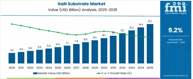
| Metric | Value |
|---|---|
| GaN Substrate Market Estimated Value in (2025 E) | USD 6.5 billion |
| GaN Substrate Market Forecast Value in (2035 F) | USD 15.7 billion |
| Forecast CAGR (2025 to 2035) | 9.2% |
The GaN Substrate market is being driven by increasing demand from sectors such as telecommunications, power electronics, and automotive applications. The current market scenario reflects growing investments in next-generation semiconductor technologies that support higher efficiency, improved thermal management, and faster switching speeds. The market’s future outlook is expected to be shaped by the continued expansion of 5G networks, electric vehicle adoption, and renewable energy infrastructure, where high-performance substrates are critical.
The transition towards more compact and energy-efficient devices has resulted in higher demand for Gallium Nitride substrates that offer superior performance over conventional materials. The market is further supported by research initiatives aimed at reducing manufacturing costs and improving yield rates.
As industries increasingly adopt energy-saving solutions, the application of GaN substrates is being expanded, paving the way for new opportunities in advanced power devices and RF systems The market is expected to witness consistent growth, driven by technological advancements and the rising focus on sustainability.
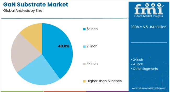
The 6-inch size segment is expected to hold 40.00% of the GaN Substrate market revenue share in 2025, making it the leading size category. The dominance of this segment is being attributed to its balanced offering between performance and manufacturing efficiency. Larger wafer sizes are being preferred as they enable higher throughput, lower cost per device, and better uniformity in semiconductor fabrication.
The widespread adoption of 6-inch substrates is being supported by growing demand in power electronics and RF applications, where efficient thermal dissipation and high-frequency operation are essential. As device integration becomes more complex, the demand for substrates that support larger die areas is being expanded.
Additionally, investments in automation and fabrication technologies have made the production of 6-inch wafers more cost-effective, encouraging manufacturers to scale up production With industry trends favoring compact and high-performance devices, the 6-inch size segment is expected to remain at the forefront of substrate offerings, supporting the broader adoption of GaN-based solutions.
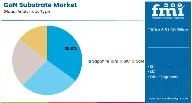
The Sapphire substrate type is projected to account for 35.00% of the GaN Substrate market revenue share in 2025, making it the largest material category. The widespread use of sapphire is being supported by its inherent properties, including high thermal conductivity, excellent electrical insulation, and compatibility with GaN epitaxial growth processes. Sapphire’s proven track record in RF and LED applications has reinforced its position as a preferred material in semiconductor fabrication.
Its stability under high temperature and ability to maintain crystalline structure during deposition processes have made it suitable for high-performance devices. The growth of this segment has also been supported by cost optimization efforts, where scaling production volumes has led to improved wafer yields and reduced manufacturing expenses.
Furthermore, the continued deployment of communication infrastructure and power devices that require reliable substrates has accelerated demand for sapphire-based solutions As industry focus on energy-efficient and high-speed devices intensifies, sapphire substrates are expected to retain their leading role, driven by their compatibility and cost-effectiveness.
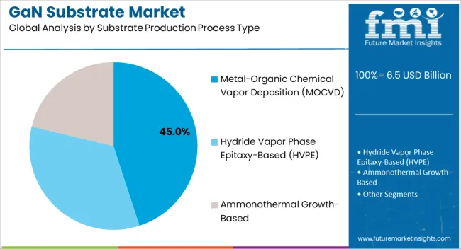
The Metal-Organic Chemical Vapor Deposition process type segment is anticipated to hold 45.00% of the GaN Substrate market revenue share in 2025, making it the dominant production process. This growth is being attributed to the process’s capability to produce high-quality epitaxial layers with uniform thickness and minimal defects. The MOCVD process supports precise control over layer composition, doping levels, and structural integrity, which are critical for high-performance semiconductor devices.
The process’s compatibility with large wafer sizes, particularly 6-inch substrates, has enabled its wide adoption in power electronics, RF systems, and optoelectronics. The scalability and repeatability of the MOCVD process have further encouraged investments in advanced fabrication facilities.
Additionally, improvements in precursor materials and reactor design have enhanced yield rates and lowered production costs, making the process more attractive for mass manufacturing With increasing demand for high-efficiency devices and stringent performance standards, the MOCVD process is expected to remain the cornerstone of GaN substrate production, driving innovation and enabling next-generation semiconductor solutions.
Wider band gap, high break-down voltage, larger critical electric field, and higher thermal conductivity are some of the major factors leading to a rapid shift of industry manufacturers from silicon technology to GaN substrate.
As these properties let the GaN Substrate material operate at much higher voltages, work at high switching frequencies, and increase its ability to handle higher power density, thereby offering enhanced power efficiency, which are the key requirements of power amplifiers and applications pertaining to optoelectronics, they are the captivating interest in the Research and Development fields of these industries.
GaN Substrate also exceeds the limit of their counterpart Si devices in applications like Schottky diodes, FETs, HEMTs, and other advanced transistors and lets them operate efficiently at much higher voltage levels.
These are the key factors that result in gaining attraction for GaN Substrate in the market, with the LED applications being the key drivers holding a share of nearly 70% of revenue in the market for the bulk gallium nitride (GaN) market.
As these devices help in reducing the conduction and switching losses and offer higher efficiency in electronic systems, gradually they are entering a new segment of applications, namely power amplifiers. These applications of GaN Substrate are in an evolving stage but are anticipated to show substantial growth in the upcoming years. All these factors are expected to accelerate the growth of the GaN Substrate Market during the forecast period.
Attributed to the compactness of car modules, the automotive and transportation industry is serving as a crucial end-use industry for the expansion of the GaN substrate market, and the ongoing undercurrents of green vehicle agendas are likely to surface new revenue streams for market players.
Besides this, as the consumer electronics industry continues to look at wafer-sized innovation to support the smart-sizing of devices, the high power-handling capacity of GaN substrates is giving these components an edge over silicon substrates.
Presently small diameters, namely 2 & 4-inch GaN substrate are present. But these are small diameters that lead to wastage of space and edges resulting in lower efficiencies. This is one of the major factors that are expected to hinder the growth of the GaN Substrates market if a large-diameter GaN Substrate is not manufactured successfully.
Additionally, some countries like USA, Japan, and Korea have started adopting large diameters, but to gain a wider acceptance of GaN Substrate may take years to come. Also, high implementation costs can result in impeding the growth of the GaN substrate market over the analysis period.
In terms of regional platforms, North America holds the largest market share in the GaN Substrate market. The region held 27.3% global market share in 2025. North America is expected to fuel the GaN Substrate market, owing to the massive advancement of technology in the region, over the forecast period.
Further, continuous innovation and development in the semiconductor industry is another growth driver of the industry in the respective region.
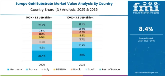
According to Future Market Insights, Europe is expected to provide immense growth opportunities for GaN Substrate since it possessed 17.2% share of the global market in 2025. Europe is expected to witness significant market growth, attributed to the increasing demand in nations such as the United Kingdom and Germany.
According to Future Market Insights, Asia-Pacific is expected to provide immense growth opportunities for the GaN substrates market. Asia-Pacific region accounts for a significant share of the GaN Substrate Market, with Japan, China, and Korea being the major contributors in the terms of production and consumption. Major factors like less labor and production costs in these countries act as catalysts in helping manufacturers to set up production facilities.
According to Future Market Insights, the Middle East & Africa are expected to provide immense growth opportunities for GaN Substrates Market. The developing GaN substrate market in the Middle East & Africa is expected to aid in the flourishing market during the forecast period.
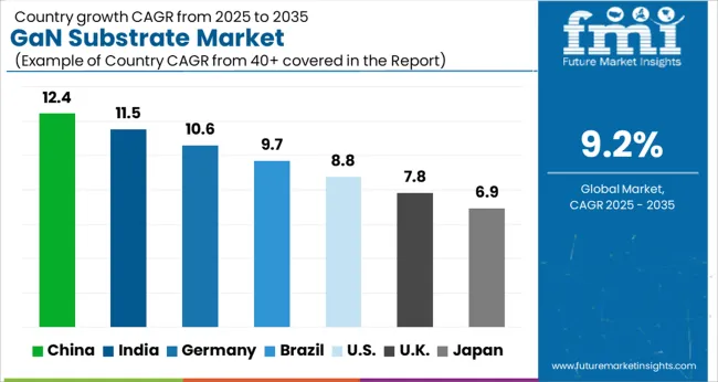
| Countries | 2025 Value Share in Global Market |
|---|---|
| United States | 15.4% |
| Germany | 8.1% |
| Japan | 5.4% |
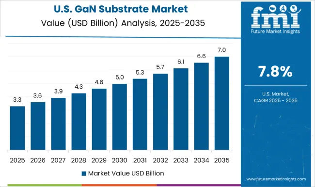
The United States GaN substrate market has grown substantially due to the increasing demand for energy-efficient devices and the rapid adoption of GaN technology across various industries. The United States is a hub for technological innovation and advancements, particularly in the semiconductor industry.
The rapid growth of the electric vehicle market in the United States directly impacts the market. GaN substrates enable efficient power conversion and higher power density. This makes them essential components for EV charging infrastructure and powertrain systems.
The deployment of 5G networks in the United States is driving the demand for GaN substrates in RF power amplifiers and base station equipment. GaN substrates provide high power efficiency and wide bandwidth. As a result, they are well-suited to high-speed data transmission in 5G networks.
Germany has a well-established research ecosystem and benefits from strong government support for technological advancements. The government's focus on fostering innovation, particularly in the fields of power electronics and telecommunications, has led to numerous research initiatives and collaborations.
This favorable environment encourages the development and commercialization of GaN substrates, fostering growth in the market. The deployment of 5G networks in Germany is creating a significant demand for GaN-based RF devices. GaN substrates enable the development of high-power and high-frequency RF components required for 5G base stations and small cells.
The country's strong focus on expanding its 5G infrastructure is expected to drive the demand for GaN substrates in the telecommunications sector.
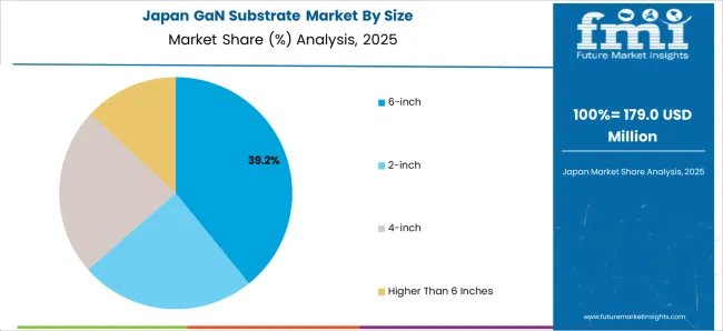
Japan has been at the forefront of GaN-on-Silicon (GaN-on-Si) technology development. GaN-on-Si substrates provide a cost-effective solution compared to traditional silicon carbide (SiC) substrates. The country's semiconductor manufacturers are investing in GaN-on-Si technology to improve device performance and reduce manufacturing costs.
This trend is expected to impact the Japan GaN substrate market positively. The automotive industry in Japan is a key driver of the GaN substrate industry. GaN-based power devices find extensive use in electric vehicles (EVs) and hybrid vehicles due to their high-power capabilities and improved efficiency. As the adoption of EVs continues to grow in Japan, the demand for GaN substrates is expected to increase significantly.
| Countries | Value CAGR (2025 to 2035) |
|---|---|
| United Kingdom | 7.2% |
| China | 7.1% |
| India | 12.1% |
The United Kingdom is witnessing significant investments in GaN-related research and development activities. Both academic institutions and private companies are actively engaged in advancing GaN substrate technologies, which is expected to drive innovation and foster market growth. The United Kingdom has increasingly focused on energy efficiency initiatives to reduce carbon emissions and achieve sustainability goals.
GaN substrates, with their superior energy efficiency and power density, are gaining traction in various sectors, including power electronics and renewable energy systems. GaN-on-Si (Gallium Nitride on Silicon) technology is gaining popularity due to its cost-effectiveness and compatibility with existing silicon manufacturing processes. This trend is expected to contribute to the growth of the United Kingdom GaN substrate market.
China's push towards renewable energy and electric vehicles has created a surge in demand for power electronics. The rapid growth of the electric vehicle market in China is driving the demand for power electronics, which, in turn, fuels the adoption of GaN substrates. The rollout of 5G networks in China has created a significant demand for high-frequency GaN-based RF devices.
China also has a robust consumer electronics industry, with a strong emphasis on innovation and product development. GaN-based devices, such as power supplies and RF components, are extensively used in smartphones, tablets, laptops, and other consumer electronics products.
The demand for high-performance and energy-efficient devices in the consumer electronics sector is driving the growth of the China GaN substrate market. Moreover, China has a well-established semiconductor manufacturing ecosystem, with several key players investing in GaN substrate production facilities.
The India GaN substrate market is poised for substantial growth. The growing need for efficient power management systems in India, coupled with the government's focus on renewable energy and electric vehicle adoption, is fueling the demand for GaN-based power electronics. With the rollout of 5G networks in India, there is a surge in demand for GaN-based radio frequency devices.
The deployment of 5G infrastructure and the need for advanced wireless communication systems are expected to drive the growth of GaN substrates in the telecommunications sector. The Indian defense and aerospace sectors are also increasingly adopting GaN-based devices for radar systems, electronic warfare, and satellite communication.
The Indian government has launched various initiatives and policies to promote the domestic semiconductor industry. Programs such as "Make in India" and "National Electronics Policy" aim to boost indigenous manufacturing and reduce dependence on imports.
| Segments | 2025 Value Share in Global Market |
|---|---|
| 2-inch GaN Substrate Size | 30.4% |
| GaN Substrate on SiC Type | 28.1% |
The dominance of the 2-inch GaN substrate segment can be attributed to several key factors. Its established technology and compatibility with existing manufacturing processes have made it a widely adopted standard in the industry. The 2-inch size strikes a balance between cost and yield, offering a larger surface area while remaining cost-effective.
It has become the preferred choice for producing GaN-based devices due to its moderate surface area, enabling economies of scale. Moreover, the market demand for GaN devices has predominantly been met by 2-inch substrates, as they provide sufficient space for device fabrication at a reasonable cost per unit.
The compatibility of the 2-inch GaN substrate with foundry services further contributes to its dominance, as many fabrication facilities offer specialized services for this size.
The GaN-on-SiC substrate segment dominates the market due to its superior material properties, well-established technology, and wide adoption in RF and power electronics. GaN-on-SiC substrates offer excellent performance, efficiency, and reliability. This is due to the combination of GaN's wide bandgap, high breakdown voltage, and high thermal conductivity.
Additionally, SiC provides a lattice match and high thermal conductivity. Together, these characteristics contribute to the superior properties of GaN-on-SiC substrates. Extensive research, development, and manufacturing investments have matured GaN-on-SiC technology, resulting in large-area substrates with low defect densities.
This technology has found significant application in RF power amplifiers, wireless base stations, radar systems, satellite communications, and power conversion devices. The demand for high-performance power electronics and RF devices across various industries has driven the growth of GaN-on-SiC substrates.
There are many prominent market players in the GaN substrate market, who are working hand-in-hand to provide the best-in-class GaN Substrates for enhancing the global arena. However, there are many global start-ups in the GaN substrate market, that are stepping forward in matching the requirements of the GaN Substrate domain.
Global Startups of GaN Substrate Market
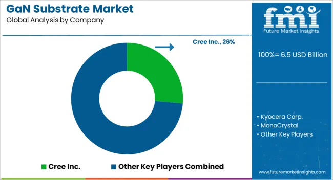
Some of the key participants present in the global GaN Substrate market include Saint Gobain/IVWorks, Sumitomo, Mitsubishi, SCIOCS, Kyocera Corp, PAM XIAMEN, Toshiba Corporation, Soitech, GaN Systems Inc., and Cree, among others.
Attributed to the presence of such a high number of participants, the market is highly competitive. While global players such as Saint Gobain/IVWorks, Sumitomo, Mitsubishi, SCIOCS, and Kyocera Corp. account for a considerable market size, several regional-level players are also operating across key growth regions.
Recent Developments
How big is the GaN substrate market in 2025?
The global GaN substrate market is estimated to be valued at USD 6.5 billion in 2025.
What will be the size of GaN substrate market in 2035?
The market size for the GaN substrate market is projected to reach USD 15.7 billion by 2035.
How much will be the GaN substrate market growth between 2025 and 2035?
The GaN substrate market is expected to grow at a 9.2% CAGR between 2025 and 2035.
What are the key product types in the GaN substrate market?
The key product types in GaN substrate market are 6-inch, 2-inch, 4-inch and higher than 6 inches.
Which type segment to contribute significant share in the GaN substrate market in 2025?
In terms of type, sapphire segment to command 35.0% share in the GaN substrate market in 2025.
Full Research Suite comprises of:
Market outlook & trends analysis
Interviews & case studies
Strategic recommendations
Vendor profiles & capabilities analysis
5-year forecasts
8 regions and 60+ country-level data splits
Market segment data splits
12 months of continuous data updates
DELIVERED AS:
PDF EXCEL ONLINE

Thank you!
You will receive an email from our Business Development Manager. Please be sure to check your SPAM/JUNK folder too.