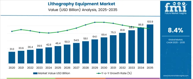
The lithography equipment market is projected to grow from USD 46.4 billion in 2025 to USD 103.9 billion in 2035, reflecting a CAGR of 8.4%. During the early adoption phase (2020–2024), the market expanded gradually from USD 31.0 billion to USD 46.4 billion as semiconductor manufacturers began investing in advanced lithography systems for higher precision and smaller node production. This period focused on pilot deployments, validating performance for next-generation chips, and addressing operational efficiency.
By 2025, the market will reach USD 46.4 billion, signaling readiness for broader adoption as production lines scale and major players increasingly standardize advanced lithography tools. Between 2025 and 2035, the market moves through scaling (2025–2030) and consolidation (2030–2035). By 2030, the market will surpass USD 64.1 billion, driven by widespread deployment in high-volume semiconductor manufacturing and expansion of production capacities. During the consolidation phase, growth continues toward USD 103.9 billion by 2035 as leading equipment suppliers dominate the market and smaller players either align with established ecosystems or exit. The 8.4% CAGR highlights steady growth, reflecting a transition from experimental adoption to broader integration, with lithography equipment becoming a critical component of mainstream semiconductor manufacturing worldwide.
| Metric | Value |
|---|---|
| Lithography Equipment Market Estimated Value in (2025 E) | USD 46.4 billion |
| Lithography Equipment Market Forecast Value in (2035 F) | USD 103.9 billion |
| Forecast CAGR (2025 to 2035) | 8.4% |
The lithography equipment market is influenced by several broader sectors, each playing a critical role in its growth. The semiconductor manufacturing market drives approximately 35%, as the scale of chip production directly affects demand for advanced lithography systems. Integrated circuit design and fabrication contribute around 20%, providing platforms and specifications that dictate equipment requirements. The wafer and substrate market accounts for 15%, supplying essential materials for lithography processes. Photomask and reticle production influences about 10%, as precision patterns are required for accurate chip patterning. Cleanroom infrastructure and facility management make up 7%, supporting operational efficiency and contamination control. Inspection and metrology systems contribute 5%, enabling quality assurance and defect detection. Chemical and photoresist suppliers account for 5%, providing the materials necessary for pattern transfer. Lastly, research and development services represent 3%, supporting innovation in process optimization and next-generation lithography solutions.
The Lithography Equipment market is experiencing steady growth driven by its critical role in semiconductor manufacturing and advanced packaging. Increasing demand for smaller, faster, and more energy-efficient integrated circuits has been driving the adoption of advanced lithography technologies. The market is being shaped by rapid innovations in extreme ultraviolet technology, improvements in optical lithography, and growing requirements for high-resolution patterning in chips used across consumer electronics, automotive, and data center applications.
The shift towards advanced packaging and multi-layer devices is encouraging manufacturers to invest in high-precision equipment capable of meeting tighter design rules. Increasing capital expenditure in semiconductor fabrication facilities, coupled with rising focus on wafer-level miniaturization and production efficiency, is supporting market growth.
In addition, the growing number of foundries and increasing adoption of AI and machine learning in semiconductor design is enhancing the demand for highly automated lithography equipment The combination of technological advancements, rising demand for high-performance chips, and continuous improvement in production efficiency is expected to sustain growth and create future opportunities in this market.
The lithography equipment market is segmented by technology, equipment, application, end use, and geographic regions. By technology, lithography equipment market is divided into Extreme Ultraviolet (EUV) Lithography, ArF, KrF, i-line, and Arf immersion. In terms of equipment, lithography equipment market is classified into Optical Lithography/Photolithography, Mask aligners, Electron beam lithography, Ion lithography, X-Ray lithography, and Nanoimprint lithography. Based on application, lithography equipment market is segmented into Advanced Packaging, MEMS devices, LED devices, and Others. By end use, lithography equipment market is segmented into Electronics Manufacturing, Healthcare and Life Sciences, Automotive Industry, Telecommunications, and Others. Regionally, the lithography equipment industry is classified into North America, Latin America, Western Europe, Eastern Europe, Balkan & Baltic Countries, Russia & Belarus, Central Asia, East Asia, South Asia & Pacific, and the Middle East & Africa.
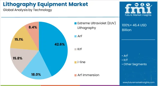
The Extreme Ultraviolet (EUV) lithography technology segment is projected to hold 42.6% of the overall market revenue in 2025, making it the leading technology type. This prominence is being attributed to the capability of EUV systems to produce extremely fine patterns at sub-10 nanometer scales, which is essential for modern semiconductor devices. Adoption has been accelerated by the increasing need for high-density memory, advanced logic chips, and next-generation processors.
The scalability and precision of EUV lithography allow wafer manufacturers to achieve higher throughput while maintaining tight tolerances, thereby reducing defect rates and overall production costs. Additionally, the capability to handle complex multi-layer architectures without compromising resolution has positioned EUV as the preferred choice for cutting-edge semiconductor fabrication.
Investment in infrastructure to support EUV systems, including advanced optics and source power enhancements, has further driven adoption As semiconductor companies continue to pursue Moore's law and develop smaller nodes, the demand for EUV lithography is expected to remain strong, reinforcing its leadership in the technology segment.

The Optical Lithography/Photolithography equipment segment is anticipated to capture 47.9% of the overall Lithography Equipment market revenue in 2025, emerging as the leading equipment type. This dominance is being driven by the long-standing reliability, cost-effectiveness, and flexibility of optical lithography systems in semiconductor manufacturing. These systems are widely used across a range of wafer sizes and device types due to their proven ability to deliver consistent patterning at mature technology nodes.
The widespread deployment of optical lithography is reinforced by its adaptability for multi-patterning techniques, which allow continued scaling without major redesign of existing production lines. The segment has also benefited from high-volume production requirements, where throughput and process stability are critical for large-scale chip fabrication.
Continuous improvements in immersion lithography and stepper/scanner technologies have enhanced resolution and performance, supporting adoption across foundries and integrated device manufacturers As demand for legacy and mid-range nodes persists, optical lithography equipment is expected to remain a cornerstone of the lithography market, ensuring cost-effective and scalable semiconductor production.
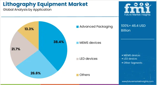
The Advanced Packaging application segment is expected to account for 38.4% of the Lithography Equipment market revenue in 2025, positioning it as the largest application area. Growth in this segment is being driven by the increasing complexity of semiconductor devices and the need for high-density, multi-layer packaging to improve performance and reduce form factor. Advanced packaging techniques, such as wafer-level packaging, system-in-package, and 3D stacking, require precise and reliable lithography equipment to pattern fine features and ensure high yield.
Adoption has been fueled by demand from high-performance computing, artificial intelligence, automotive electronics, and 5G communications, where devices must meet stringent performance and thermal requirements. The integration of lithography into advanced packaging workflows allows manufacturers to achieve smaller interconnect pitches and enhanced electrical performance without significant increases in cost or processing time.
Rising investments in semiconductor manufacturing infrastructure, coupled with the push for miniaturized and energy-efficient devices, are expected to sustain growth in the advanced packaging application segment This segment is anticipated to remain a critical driver of revenue for lithography equipment providers as technology evolves.
The lithography equipment market is expanding due to increasing semiconductor demand, miniaturization of integrated circuits, and rising adoption of advanced fabrication technologies. North America and Europe lead in high-precision, extreme ultraviolet (EUV) and deep ultraviolet (DUV) lithography systems for cutting-edge chip manufacturing. Asia-Pacific shows rapid growth driven by semiconductor manufacturing expansion, foundries, and electronics production. Manufacturers differentiate through resolution capability, throughput, defect control, and automation. Regional variations in R&D investment, semiconductor ecosystem maturity, and cost sensitivity influence adoption, deployment strategies, and competitive positioning globally.
High-resolution capability and wafer throughput are critical for lithography equipment adoption. North America and Europe emphasize EUV and advanced DUV systems capable of sub-5nm node fabrication for high-performance computing and AI chips, requiring precise alignment, defect-free exposure, and rapid processing speed. Asia-Pacific markets increasingly adopt DUV and mid-range lithography tools for mass-market electronics and consumer devices, balancing cost and performance. Differences in resolution and throughput affect fabrication efficiency, yield, and overall production capacity. Leading suppliers invest heavily in advanced optics, laser sources, and automation, while regional players focus on reliable, cost-efficient equipment. Resolution and throughput contrasts shape adoption patterns, product differentiation, and competitiveness across global semiconductor fabrication sectors.
Reliability, uptime, and maintenance requirements strongly influence lithography equipment adoption. North America and Europe prioritize high-reliability systems with predictive maintenance, remote diagnostics, and long operational lifespans to ensure continuous wafer production and minimize downtime in semiconductor fabs. Asia-Pacific manufacturers implement similar solutions for high-volume production but often rely on modular and serviceable systems to control costs. Differences in reliability and maintenance impact productivity, operating costs, and equipment ROI. Suppliers providing robust, low-downtime lithography tools gain higher adoption, while regional producers focus on scalable, service-friendly designs. Reliability and maintenance contrasts shape adoption, operational efficiency, and competitiveness across semiconductor manufacturing globally.
Successful adoption depends on seamless integration with wafer fabrication processes, photomasks, and metrology tools. North America and Europe emphasize ecosystem compatibility for EUV and advanced nodes, integrating lithography equipment with automation systems, fab software, and inspection platforms. Asia-Pacific adoption focuses on mid-range fabrication environments with standardized process flows, balancing integration complexity and cost. Differences in integration affect throughput, defect management, and process efficiency. Suppliers providing fully compatible, end-to-end integrated systems gain premium adoption, while regional players offer modular, adaptable tools. Integration contrasts shape market penetration, operational efficiency, and strategic positioning in the global lithography equipment industry.
Environmental compliance, safety regulations, and energy efficiency standards significantly influence lithography equipment deployment. North America and Europe enforce strict requirements for energy consumption, chemical handling, and emissions in semiconductor fabs, influencing equipment design and operational costs. Asia-Pacific regulations vary, with advanced fabs adhering to global standards, while emerging regions implement locally defined compliance measures. Differences in regulatory requirements affect procurement approval, equipment design modifications, and operating procedures. Suppliers providing compliant, energy-efficient systems gain market credibility and higher adoption rates, while regional manufacturers focus on affordable, compliant solutions. Regulatory contrasts shape adoption, sustainability, and competitive positioning across global lithography equipment markets.
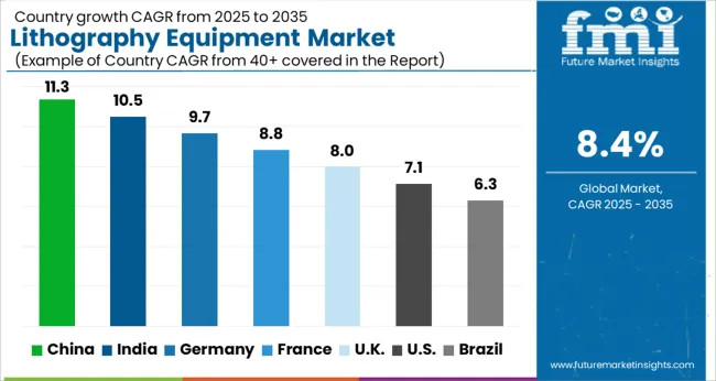
| Country | CAGR |
|---|---|
| China | 11.3% |
| India | 10.5% |
| Germany | 9.7% |
| France | 8.8% |
| UK | 8.0% |
| USA | 7.1% |
| Brazil | 6.3% |
The global lithography equipment market was projected to grow at an 8.4% CAGR through 2035, driven by demand in semiconductor manufacturing, microelectronics, and precision fabrication applications. Among BRICS nations, China recorded 11.3% growth as large-scale production and assembly facilities were commissioned and compliance with industrial and safety standards was enforced, while India at 10.5% growth saw expansion of manufacturing units to meet rising regional demand. In the OECD region, Germany at 9.7% maintained substantial output under strict industrial and operational regulations, while the United Kingdom at 8.0% relied on moderate-scale operations for semiconductor and microfabrication applications. The USA, expanding at 7.1%, remained a mature market with steady demand across commercial and industrial microelectronics segments, supported by adherence to federal and state-level quality and safety standards. This report includes insights on 40+ countries; the top five markets are shown here for reference.
The lithography equipment market in China is growing at a CAGR of 11.3% due to the rapid development of semiconductor manufacturing and electronics industries. Companies are investing in advanced photolithography systems for wafer fabrication, microchips, and display technologies. Government initiatives supporting domestic semiconductor production and high tech manufacturing encourage adoption. Manufacturers are emphasizing high precision, automation, and energy efficiency in equipment design to meet industrial demands. Distribution through authorized suppliers, OEMs, and service providers ensures accessibility for both industrial and research applications. Growing demand from electronics, automotive, and communication sectors is driving market growth. Research and development in higher resolution, faster, and reliable systems is accelerating innovation. China is emerging as a global leader in lithography equipment due to its large semiconductor industry and strong manufacturing ecosystem.
Lithography equipment market is expanding at a CAGR of 10.5% in India with rising semiconductor and electronics manufacturing activity. Companies are adopting advanced photolithography tools for wafer processing, microchip fabrication, and display technology production. Government programs promoting electronics manufacturing, semiconductor self reliance, and research infrastructure support market growth. Manufacturers focus on energy efficient, automated, and high precision systems to meet industrial requirements. Distribution through OEMs and authorized suppliers ensures accessibility across both industrial and research applications. Demand is further driven by the electronics, automotive, and telecommunication sectors. India’s increasing investments in semiconductor infrastructure and R&D are supporting steady adoption of lithography equipment.
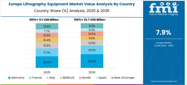
Lithography equipment market in Germany is growing at a CAGR of 9.7% supported by strong demand from advanced semiconductor, electronics, and automotive industries. Companies are deploying high precision photolithography systems for wafer fabrication and microchip production. Manufacturers focus on automation, high resolution, and energy efficiency to meet stringent industrial standards. Distribution through OEMs and service partners ensures accessibility for industrial and research purposes. Growth is fueled by strong R&D investment, environmental and efficiency standards, and increasing demand for electronic devices. Germany’s advanced semiconductor ecosystem and focus on precision manufacturing are key factors driving adoption of lithography equipment in both industrial and research applications.
The United Kingdom market is expanding at a CAGR of 8.0% with adoption of lithography equipment in semiconductor, electronics, and research sectors. Manufacturers are offering high performance, automated, and energy efficient photolithography tools for wafer processing, microchip fabrication, and display technology. Distribution through OEMs, suppliers, and service providers ensures accessibility. Increasing demand for microchips, electronics devices, and high tech R&D drives market growth. Companies are focusing on precision, reliability, and process optimization to enhance production efficiency. Government initiatives supporting semiconductor research and high tech manufacturing contribute to adoption. The United Kingdom is witnessing steady growth in lithography equipment for both industrial and research applications.
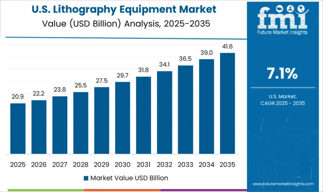
The United States market is growing at a CAGR of 7.1% due to strong adoption of lithography equipment in semiconductor and electronics manufacturing. Manufacturers are deploying automated, high precision, and energy efficient systems for wafer fabrication, microchip production, and display technologies. Distribution through OEMs, authorized suppliers, and service providers ensures availability for both industrial and research applications. Growth is driven by increasing demand for electronic devices, automotive electronics, and research projects. Manufacturers are focusing on higher resolution, faster processing, and operational reliability. Federal and private investments in semiconductor technology and electronics R&D support market adoption. The United States remains a key global market for lithography equipment due to technological readiness, strong semiconductor ecosystem, and high demand from multiple industries.
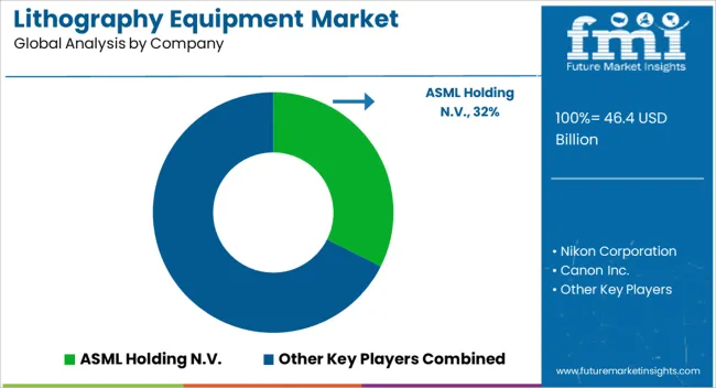
The lithography equipment market is a cornerstone of semiconductor manufacturing, enabling the precise patterning of microchips and advanced electronic devices. Leading suppliers in this market include ASML Holding N.V., Nikon Corporation, Canon Inc., Veeco Instruments Inc., SUSS MicroTec AG, EV Group, SCREEN Holdings Co., Ltd., Onto Innovation Inc., JEOL Ltd, Neutronix Quintel Inc. (NXQ), Advantest, and Shanghai Micro Electronics Equipment (Group) Co., Ltd.. These companies focus on developing high-precision photolithography systems, nanoimprint technologies, and semiconductor inspection tools that are critical for advanced node semiconductor production and next-generation chip designs. ASML Holding N.V. dominates the market with its extreme ultraviolet (EUV) lithography systems, enabling the production of smaller, more efficient, and higher-performing semiconductor devices. Nikon Corporation and Canon Inc. continue to innovate in immersion lithography and stepper technologies, catering to high-volume semiconductor fabrication plants. Veeco Instruments Inc., SUSS MicroTec AG, and EV Group specialize in wafer bonding, nanoimprint, and photolithography process solutions, supporting advanced packaging and MEMS device production. Other key players like SCREEN Holdings Co., Ltd., Onto Innovation Inc., JEOL Ltd, and NXQ focus on semiconductor inspection, metrology, and electron-beam lithography systems, ensuring high yield, precision, and process reliability. Advantest offers integrated lithography test and inspection solutions, while Shanghai Micro Electronics Equipment (Group) Co., Ltd. emphasizes cost-effective and scalable lithography equipment for emerging semiconductor markets in Asia. The market is driven by the continuous demand for miniaturized, high-performance chips in applications such as artificial intelligence, 5G, automotive electronics, and IoT devices. These leading suppliers are investing heavily in research and development to push the limits of patterning resolution, throughput, and process automation, maintaining their competitive edge in a rapidly evolving semiconductor landscape.
| Item | Value |
|---|---|
| Quantitative Units | USD 46.4 Billion |
| Technology | Extreme Ultraviolet (EUV) Lithography, ArF, KrF, i-line, and Arf immersion |
| Equipment | Optical Lithography/Photolithography, Mask aligners, Electron beam lithography, Ion lithography, X-Ray lithography, and Nanoimprint lithography |
| Application | Advanced Packaging, MEMS devices, LED devices, and Others |
| End Use | Electronics Manufacturing, Healthcare and Life Sciences, Automotive Industry, Telecommunications, and Others |
| Regions Covered | North America, Europe, Asia-Pacific, Latin America, Middle East & Africa |
| Country Covered | United States, Canada, Germany, France, United Kingdom, China, Japan, India, Brazil, South Africa |
| Key Companies Profiled | ASML Holding N.V., Nikon Corporation, Canon Inc., Veeco Instruments Inc., SUSS MicroTec AG, EV Group, SCREEN Holdings Co., Ltd., Onto Innovation Inc., JEOL Ltd, Neutronix Quintel Inc. (NXQ), Advantest, and Shanghai Micro Electronics Equipment (Group) Co., Ltd. |
| Additional Attributes | Dollar sales vary by equipment type, including steppers, scanners, and mask aligners; by technology, such as photolithography, extreme ultraviolet (EUV), and electron beam lithography; by application, spanning semiconductor manufacturing, MEMS, and microelectronics; by end-use industry, covering semiconductor fabs, research labs, and electronics manufacturing; by region, led by North America, Europe, and Asia-Pacific. Growth is driven by rising semiconductor demand, miniaturization, and advanced chip fabrication needs. |
The global lithography equipment market is estimated to be valued at USD 46.4 billion in 2025.
The market size for the lithography equipment market is projected to reach USD 103.9 billion by 2035.
The lithography equipment market is expected to grow at a 8.4% CAGR between 2025 and 2035.
The key product types in lithography equipment market are extreme ultraviolet (euv) lithography, arf, krf, i-line and arf immersion.
In terms of equipment, optical lithography/photolithography segment to command 47.9% share in the lithography equipment market in 2025.
Our Research Products

The "Full Research Suite" delivers actionable market intel, deep dives on markets or technologies, so clients act faster, cut risk, and unlock growth.

The Leaderboard benchmarks and ranks top vendors, classifying them as Established Leaders, Leading Challengers, or Disruptors & Challengers.

Locates where complements amplify value and substitutes erode it, forecasting net impact by horizon

We deliver granular, decision-grade intel: market sizing, 5-year forecasts, pricing, adoption, usage, revenue, and operational KPIs—plus competitor tracking, regulation, and value chains—across 60 countries broadly.

Spot the shifts before they hit your P&L. We track inflection points, adoption curves, pricing moves, and ecosystem plays to show where demand is heading, why it is changing, and what to do next across high-growth markets and disruptive tech

Real-time reads of user behavior. We track shifting priorities, perceptions of today’s and next-gen services, and provider experience, then pace how fast tech moves from trial to adoption, blending buyer, consumer, and channel inputs with social signals (#WhySwitch, #UX).

Partner with our analyst team to build a custom report designed around your business priorities. From analysing market trends to assessing competitors or crafting bespoke datasets, we tailor insights to your needs.
Supplier Intelligence
Discovery & Profiling
Capacity & Footprint
Performance & Risk
Compliance & Governance
Commercial Readiness
Who Supplies Whom
Scorecards & Shortlists
Playbooks & Docs
Category Intelligence
Definition & Scope
Demand & Use Cases
Cost Drivers
Market Structure
Supply Chain Map
Trade & Policy
Operating Norms
Deliverables
Buyer Intelligence
Account Basics
Spend & Scope
Procurement Model
Vendor Requirements
Terms & Policies
Entry Strategy
Pain Points & Triggers
Outputs
Pricing Analysis
Benchmarks
Trends
Should-Cost
Indexation
Landed Cost
Commercial Terms
Deliverables
Brand Analysis
Positioning & Value Prop
Share & Presence
Customer Evidence
Go-to-Market
Digital & Reputation
Compliance & Trust
KPIs & Gaps
Outputs
Full Research Suite comprises of:
Market outlook & trends analysis
Interviews & case studies
Strategic recommendations
Vendor profiles & capabilities analysis
5-year forecasts
8 regions and 60+ country-level data splits
Market segment data splits
12 months of continuous data updates
DELIVERED AS:
PDF EXCEL ONLINE
Equipment Management Software Market Size and Share Forecast Outlook 2025 to 2035
Equipment cases market Size and Share Forecast Outlook 2025 to 2035
EUV Lithography Market Size and Share Forecast Outlook 2025 to 2035
Farm Equipment Market Forecast and Outlook 2025 to 2035
Golf Equipment Market Size and Share Forecast Outlook 2025 to 2035
Port Equipment Market Size and Share Forecast Outlook 2025 to 2035
Pouch Equipment Market Growth – Demand, Trends & Outlook 2025 to 2035
Garage Equipment Market Forecast and Outlook 2025 to 2035
Mining Equipment Industry Analysis in Latin America Size and Share Forecast Outlook 2025 to 2035
Subsea Equipment Market Size and Share Forecast Outlook 2025 to 2035
Pavers Equipment Market Size and Share Forecast Outlook 2025 to 2035
Tennis Equipment Market Analysis - Size, Share, and Forecast Outlook 2025 to 2035
Galley Equipment Market Analysis and Forecast by Fit, Application, and Region through 2035
Sorting Equipment Market Size and Share Forecast Outlook 2025 to 2035
General Equipment Rental Services Market Size and Share Forecast Outlook 2025 to 2035
Stencil Lithography Market Size and Share Forecast Outlook 2025 to 2035
Bagging Equipment Market Size and Share Forecast Outlook 2025 to 2035
RF Test Equipment Market Size and Share Forecast Outlook 2025 to 2035
Medical Equipment Covers Market Size and Share Forecast Outlook 2025 to 2035
Telecom Equipment Market Size and Share Forecast Outlook 2025 to 2035

Thank you!
You will receive an email from our Business Development Manager. Please be sure to check your SPAM/JUNK folder too.
Chat With
MaRIA